background image

1-8-1

HM240FIS

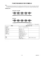
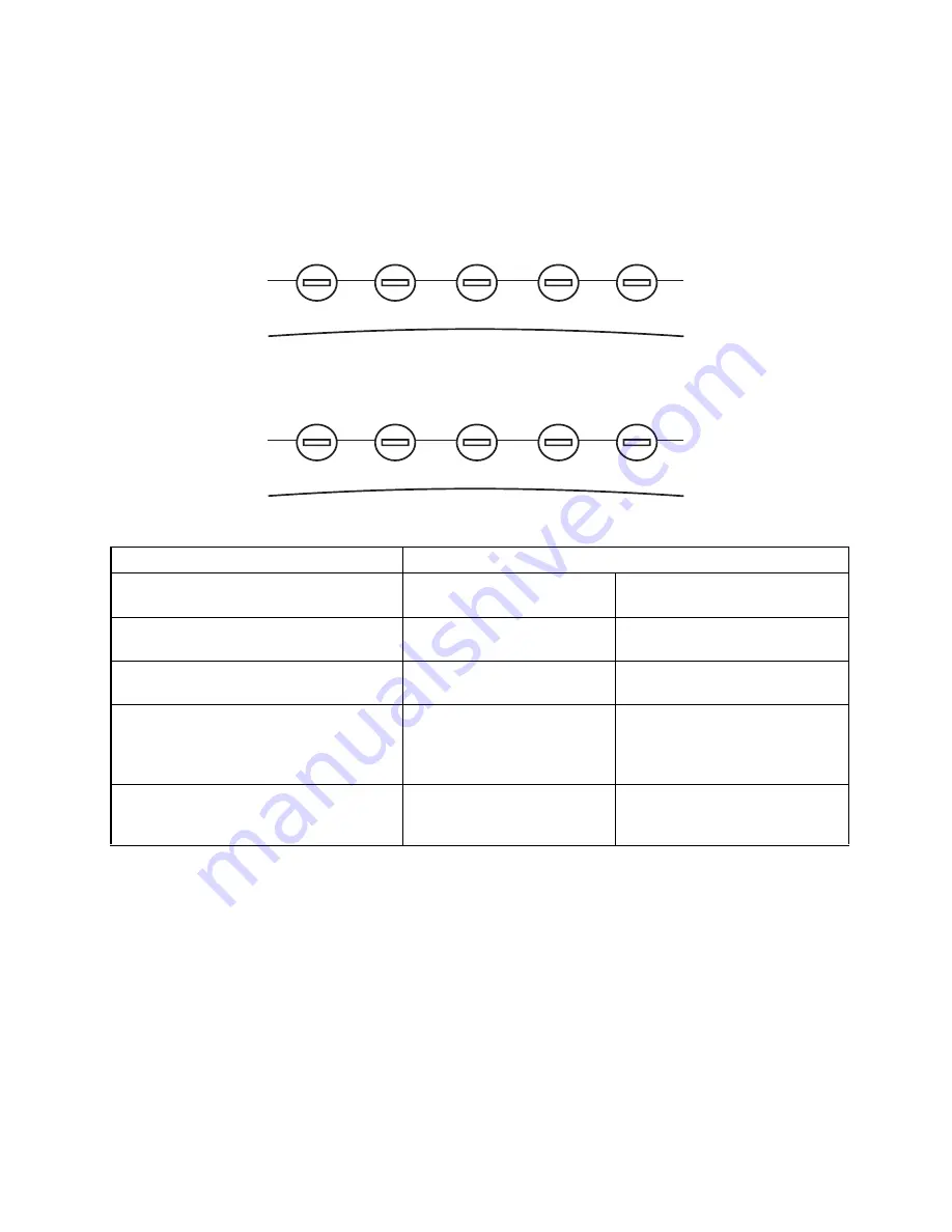
FUNCTION INDICATOR SYMBOLS

Note:

The following symbols will appear on the indicator panel to indicate the current mode or operation of the VCR.
On-screen modes will also be momentarily displayed on the tv screen when you press the operation buttons. 

Display panel

" H "= LED Light on,  " L "= LED Light off

MODE

INDICATOR ACTIVE

STANDBY
VEILLE

Always " H " during electricity

FUNCTION
FONCTION

Power on = " H "
Power off = " L "

TAPE IN
CASSETTE

Cassette in = " H " 
Cassette out = " L "

TIMER
MINUTERIE

Timer stand by = " H " 
One touch recording = " H "
Timer recording = " H "
General mode = " L " 

REC
ENR.

REC mode = " H "
REC pause 
General mode = " L "

Blinks at 0.8Hz interval

TAPE IN

TIMER

REC

FUNCTION

STANDBY

31A-250 / 31D-250

31C-250

CASSETTE

MINUTERIE

ENR. 

FONCTION

VEILLE

Summary of Contents for 31A-250

Page 1: ...Adjustment Procedures I Schematic Diagrams I CBA s I Exploded views I Parts List When servicing the deck mechanism refer to MK14 Deck Mechanism Section Deck Mechanism Part No 31A 250 31D 250 N25A0FL 31C 250 N25A1FL VIDEO CASSETTE RECORDER SECAM PAL 31A 250 31D 250 31C 250 PAL ...

Page 2: ...ons 1 6 1 How to Initialize the VCR 1 7 1 Function Indicator Symbols 1 8 1 Block Diagrams 1 9 1 Schematic Diagrams CBA s and Test Points 1 10 1 Waveforms 1 11 1 Wiring Diagrams 1 12 1 IC Pin Function Descriptions 1 13 1 Lead Identifications 1 14 1 Exploded Views 1 15 1 Mechanical Parts List 1 16 1 Electrical Parts List 1 17 1 Sec 1 Main Section I Specifications I Preparation for Servicing I Adjust...

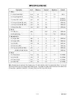
Page 3: ... Vp p 0 8 1 0 1 2 1 3 Video S N Y R P dB 40 45 SP Mode W O Burst 1 4 Video Color S N AM R P dB 37 41 SP Mode 1 5 Video Color S N PM R P dB 30 36 SP Mode 1 6 Resolution PB Line 230 245 SP Mode 2 Servo 2 1 Jitter Low µsec 0 07 0 12 SP Mode 2 2 Wow Flutter 0 3 0 5 SP Mode 3 Normal Audio 3 1 Output PB dBV 9 6 3 SP Mode 3 2 Output R P dBV 9 6 1 5 SP Mode 3 3 S N R P dB 36 41 SP Mode 3 4 Distortion R P ...

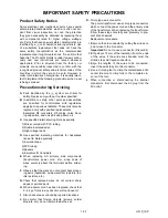
Page 4: ... especially 1 Wires covered with PVC tubing 2 Double insulated wires 3 High voltage leads D Use specified insulating materials for hazardous live parts Note especially 1 Insulation tape 2 PVC tubing 3 Spacers 4 Insulators for transistors E When replacing AC primary side components transformers power cord etc wrap ends of wires securely about the terminals before solder ing F Observe that the wires...

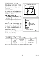
Page 5: ...ts RF termi nals antenna terminals video and audio input and output terminals microphone jacks earphone jacks etc is lower than or equal to the specified value in the table below Measuring Method Power ON Insert load Z between B earth ground power cord plug prongs and exposed accessible parts Use an AC voltmeter to measure across the terminals of load Z See Fig 2 and the following table AC Line Vo...

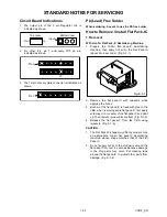
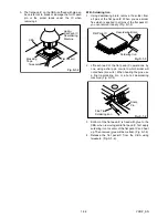
Page 6: ...e flat pack IC with tweezers while applying the hot air 3 Bottom of the flat pack IC is fixed with glue to the CBA when removing entire flat pack IC first apply soldering iron to center of the flat pack IC and heat up Then remove glue will be melted Fig S 1 6 4 Release the flat pack IC from the CBA using tweezers Fig S 1 6 CAUTION 1 The Flat Pack IC shape may differ by models Use an appropriate ho...

Page 7: ... by one using a sharp pin or wire to which solder will not adhere iron wire When heating the pins use a fine tip soldering iron or a hot air desoldering machine Fig S 1 4 3 Bottom of the flat pack IC is fixed with glue to the CBA when removing entire flat pack IC first apply soldering iron to center of the flat pack IC and heat up Then remove glue will be melted Fig S 1 6 4 Release the flat pack I...

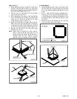
Page 8: ...rs Fig S 1 6 Note When using a soldering iron care must be taken to ensure that the flat pack IC is not being held by glue When the flat pack IC is removed from the CBA handle it gently because it may be damaged if force is applied 2 Installation 1 Using desoldering braid remove the solder from the foil of each pin of the flat pack IC on the CBA so you can install a replacement flat pack IC more e...

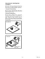
Page 9: ...ed to remove any static electricity that may be charged on the body 2 Ground for Workbench Be sure to place a conductive sheet or copper plate with proper grounding 1 MΩ on the workbench or other surface where the semi conductors are to be placed Because the static electricity charge on clothing will not escape through the body grounding band be careful to avoid contacting semi conductors with you...

Page 10: ...into the Deck Mechanism Assembly and press the PLAY button The tape will be loaded into the Deck Mechanism Assembly Make sure the power is on connect TP507 S INH to GND This will stop the function of Tape Start Sensor Tape End Sensor and Reel Sensors If these TPs are connected before plugging in the unit the function of the sensors will stay valid See Fig 1 Note Because the Tape End Sensors are in...

Page 11: ...fragile Be careful not to break them 1 Remove five Screws S 2 three Screws S 3 and Screw S 4 Then slowly lift the VCR Chassis Unit Deck Assembly Jack CBA and Main CBA up 2 When reassembling solder wire jumpers as shown in Fig D5 3 Before installing the Deck Assembly be sure to place the pin of LD SW on Main CBA as shown in Fig D6 Then install the Deck Assembly while aligning the hole of Cam Gear w...

Page 12: ...1 5 2 HM340DC Fig D2 L 2 L 1 2 Front Assembly L 2 Fig D3 S 2 S 2 S 4 S 2 S 2 S 3 S 3 3 VCR Chassis Unit Fig D4 S 5 4 Jack CBA Desolder ...

Page 13: ...rom Cylinder Assembly From ACE Head Assembly Lead with white stripe Lead with blue stripe Desolder from bottom Lead with blue stripe From Capstan Motor Assembly Lead connections of Deck Assembly and Main CBA Printing side TOP VIEW Fig D5 Fig D6 6 Main CBA SW507 LD SW LD SW Pin Hole Hole Shaft Cam Gear 6 Main CBA 5 Deck Assembly Pin ...

Page 14: ...scope Dual trace with 10 1 probe V Range 0 001 50V Div F Range DC AC 20MHz 2 Alignment Tape FL6A Head Switching Position Adjustment Purpose To determine the Head Switching position during playback Symptom of Misadjustment May cause Head Switching noise or vertical jitter in the picture Reference Notes Playback the Alignment tape and adjust VR501 so that the V sync front edge of the CH1 video outpu...

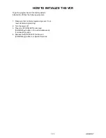
Page 15: ...CR as the following procedure 1 Make sure that no timer programming is set If not reset all timer programming 2 Turn the power off 3 Press the STOP EJECT button and CHANNEL K button on the unit simultaneously for at least 2 seconds 4 Release the STOP EJECT button and CHANNEL K button to complete this mode ...

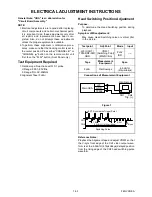
Page 16: ...ttons Display panel H LED Light on L LED Light off MODE INDICATOR ACTIVE STANDBY VEILLE Always H during electricity FUNCTION FONCTION Power on H Power off L TAPE IN CASSETTE Cassette in H Cassette out L TIMER MINUTERIE Timer stand by H One touch recording H Timer recording H General mode L REC ENR REC mode H REC pause General mode L Blinks at 0 8Hz interval TAPE IN TIMER REC FUNCTION STANDBY 31A 2...

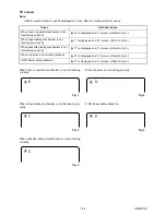
Page 17: ...ction Cause Indicator Active When reel or capstan mechanism is not functioning correctly A R is displayed on a TV screen Refer to Fig 1 When tape loading mechanism is not functioning correctly A T is displayed on a TV screen Refer to Fig 2 When cassette loading mechanism is not functioning correctly A C is displayed on a TV screen Refer to Fig 3 When the drum is not working properly A D is display...

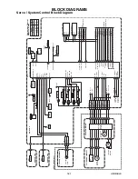
Page 18: ... VIDEO BLOCK TO AUDIO BLOCK SDA SDA SCL SCL TU701 TUNER UNIT IC503 MEMORY 72 83 IIC BUS SCL D V SYNC D REC H RF SW C ROTA IIC BUS SDA V ENV C SYNC IIC BUS SCL 71 3 5 SDA SCL 12 11 LD SW 9 AL 12V 20 5V P ON 15V AL 5V AL 5V SW507 AL 12V P ON 5V LD SW AL 5V D502 S LED FROM TO POWER SUPPLY BLOCK KEY SWITCH KEY SWITCH TP507 SENS INH IC501 SERVO SYSTEM CONTROL AUDIO SW 1 29 AUDIO SW 2 30 AUDIO SW 1 AUDI...

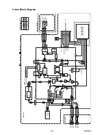
Page 19: ... 1 VIDEO IN2 3 1 3 JACK CBA 48 50 52 56 24 6 50 52 19 20 JK101 VIDEO OUT1 VIDEO IN1 19 20 JK102 CN151 CN152 CN101 CN102 VIDEO OUT2 VIDEO IN2 61 63 96 95 93 94 CHARA INS CCD 1H DELAY SP BYPASS MUTE PB EE IN1 TUNER IN1 TUNER MUTE PB EE IN2 IN2 AGC P R R Y C P R P R P EP Y DELAY Y C MIX 21 79 78 AGC VXO OSD CHARACTER MIX FBC 1 2 58 59 65 29 28 IIC BUS SDA IIC BUS SCL 69 68 46 43 67 84 62 70 D REC H 8...

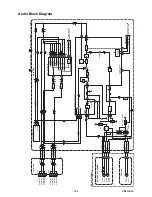
Page 20: ...M 6 AE H 5 AE H FE H AUDIO HEAD AUDIO ERASE HEAD ACE HEAD ASSEMBLY FE HEAD 2 FE H 1 FE H GND CN501 MAIN CBA PB AUDIO SIGNAL REC AUDIO SIGNAL Mode SP REC 71 A MUTE H AUDIO SW 1 AUDIO SW 2 IIC BUS SCL IIC BUS SDA TO SERVO SYSTEM CONTROL BLOCK TO SERVO SYSTEM CONTROL BLOCK FULL ERASE HEAD 68 69 SERIAL DECODER DECK ASSEMBLY 12 16 INV ATT AUDIO IN1 AUDIO OUT1 7 5 JACK CBA JK101 CN101 AUDIO IN2 AUDIO OU...

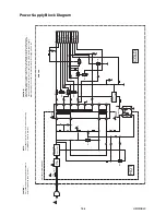
Page 21: ... 18 T1 6A L 250V Q055 Q059 SHUNT REGULATOR CAUTION Fixed voltage or Auto voltage selectable power supply circuit is used in this unit If Main Fuse F001 is blown check to see that all components in the power supply circuit are not defective before you connect the AC plug to the AC power supply Otherwise it may cause some components in the power supply circuit to fail NOTE The voltage for parts in h...

Page 22: ...itute replacement parts that do not have the same safety characteristics as specified in the parts list may create shock fire or other hazards Notes 1 Do not use the part number shown on these draw ings for ordering The correct part number is shown in the parts list and may be slightly different or amended since these drawings were prepared 2 All resistance values are indicated in ohms K 103 M 106...

Page 23: ...in original function and reliability of repaired units use only original replacement parts which are listed with their part numbers in the parts list section of the service manual 4 Mode SP REC 5 Voltage indications for PLAY and REC modes on the schematics are as shown below 6 How to read converged lines 7 Test Point Information 2 3 1 5 0 2 5 PLAY mode REC mode 5 0 The same voltage for both PLAY R...

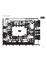
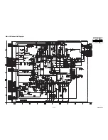
Page 24: ...1 10 3 HM240SCM1 Main 1 6 Schematic Diagram Comparison Chart of Models and Marks MODEL MARK 31A 250 A 31C 250 B 31D 250 C ...

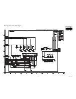
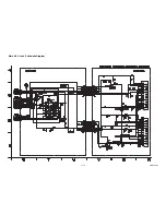
Page 25: ...1 10 4 HM240SCM2 Main 2 6 Sensor Schematic Diagram Comparison Chart of Models and Marks MODEL MARK 31A 250 A 31C 250 B 31D 250 C ...

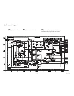
Page 26: ...1 10 5 HM240SCM3 Main 3 6 Schematic Diagram Comparison Chart of Models and Marks MODEL MARK 31A 250 A 31C 250 B 31D 250 C ...

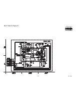
Page 27: ...1 10 6 HM240SCM4 Main 4 6 Jack Schematic Diagram ...

Page 28: ... fire hazard replace only with the same type fuse CAUTION Fixed voltage or Auto voltage selectable power supply circuit is used in this unit If Main Fuse F001 is blown check to see that all components in the power supply circuit are not defective before you connect the AC plug to the AC power supply Otherwise it may cause some components in the power supply circuit to fail ...

Page 29: ...1 10 8 HM242SCM6 Main 6 6 Schematic Diagram B Comparison Chart of Models and Marks MODEL MARK 31A 250 A 31C 250 B 31D 250 C ...

Page 30: ...t is used in this unit If Main Fuse F001 is blown check to see that all components in the power supply circuit are not defective before you connect the AC plug to the AC power supply Otherwise it may cause some components in the power supply circuit to fail Because a hot chassis ground is present in the power supply circut an isolation transformer must be used Also in order to have the ability to ...

Page 31: ...is unit If Main Fuse F001 is blown check to see that all components in the power supply circuit are not defective before you connect the AC plug to the AC power supply Otherwise it may cause some components in the power supply circuit to fail Because a hot chassis ground is present in the power supply circut an isolation transformer must be used Also in order to have the ability to increase the in...

Page 32: ...1 10 11 BHM450F01011C Jack CBA Top View Jack CBA Bottom View ...

Page 33: ...OLOR BAR SIGNAL WITH 1KHz AUDIO SIGNAL WF1 WF3 WF3 V OUT E E 10µs 50mV x 10 J23 WF3 UPPER WF1 LOWER V OUT 0 1V x 10 RF SW 0 5V x 10 50µs J23 TP502 WF2 C PB 10mV x 10 RF SW 0 5V x 10 5ms UPPER LOWER WF1 TP502 TP301 1 11 1 U31PWF ...

Page 34: ... 2 FE H GND 1 CN501 CN502 CN504 CN253 GND 1 VIDEO OUT1 2 AL 12V 1 3 VIDEO IN1 4 AUDIO OUT1 5 JK1 8P OUT 6 AUDIO IN1 7 1 2 3 4 5 6 7 CN151 CN101 FULL ERASE HEAD FE HEAD VIDEO R HEAD VIDEO L HEAD GND 1 VIDEO OUT2 2 NU 3 VIDEO IN2 4 GND 5 AUDIO OUT2 6 SC2 IN 7 AUDIO IN2 8 1 2 3 4 5 6 7 8 CN152 CN102 AC CORD ANT IN ANT OUT MAIN CBA 1 2 3 4 5 6 7 8 9 10 11 12 13 14 15 16 17 18 19 20 21 JACK CBA JK101 1...

Page 35: ...utput H Hi z 14 IN REMOCON IN Remote Control Sensor L 15 OUT C ROTA Color Phase Rotary Changeover SIgnal H L 16 NU Not Used 17 NU Not Used 18 OUT RF SW Video Head Switching Pulse H L 19 NU Not Used 20 NU Not Used 21 NU Not Used 22 A B NU Not Used C OUT TUN SW2 Tuner System Control Signal Output H L 23 OUT POWER LED STANDBY LED Signal Output H 24 OUT CAS LED TAPE IN LED Signal Output H 25 OUT TIMER...

Page 36: ...UT Signal Name Function Active Level 65 A C NU Not Used B OUT TRICK H Special Playback H in SECAM Mode H 65 NU Not Used 66 OUT C POW SW Capstan Power Switching Signal H L 67 OUT P ON H Power On Signal at High H 68 NU Not Used 69 NU Not Used 70 NU Not Used 71 OUT IIC BUS SCL I2 C BUS Control Clock H L 72 IN OUT IIC BUS SDA I2 C BUS Control Data H L 73 NU Not Used 74 NU Not Used 75 NU Not Used 76 OU...

Page 37: ...2 AMPVRE Fin V Ref for CTL AMP 93 P80 C P80 C Terminal 94 IN OUT CTL Playback Record Control Signal H L 95 IN OUT CTL Playback Record Control Signal H L 96 AMPC CTL AMP Connected Terminal 97 CTLAMP out To Monitor for CTL AMP Output PULSE 98 AMPVcc AMPVcc 99 AVcc A D Converter Power Input Standard Voltage Input 100 IN AGC IF AGC Comparator Signal A D Pin No Mark IN OUT Signal Name Function Active L...

Page 38: ...RA103M AT P KRC103M AT P KTA 1266 GR AT P KTA1267 GR Y AT P KTC3199 BL GR Y AT P RN2204 TE4 F T 2SA1015 GR TE2 F T 2SA1020 Y TE6 F M 2SC1815 BL GR Y TE2 F T 2SC2120 Y TE2 F T KTA1281Y AT P KTC3203 Y AT P BR24L02F WE2 CAT24WC02WI TE13 2SK3566 FMG4A T148 RN1511 TE85R F Note A Anode K Cathode E Emitter C Collector B Base R Reference S Source G Gate D Drain MID 32A22F PT204 6B 12 KTA1504S GR Y RTK P K...

Page 39: ...1 15 1 HM340FEX EXPLODED VIEWS Front Panel A1X ...

Page 40: ...bers are not in sequence 2B18 A2 2L011 2L011 2L011 2L011 2L011 2B9 2B9 2L022 2L022 2L012 JACK CBA A5 2L041 A10 2L031 2L099 2L041 2B7 SENSOR CBA 2B8 2B46 A7 A3 2L042 2L021 2L021 2L021 2L021 2L021 2B5 2L051 1B1 MAIN CBA Comparison Chart of Models and Marks Model Mark 31A 250 31C 250 31D 250 A B C ...

Page 41: ... NO Some Ref Numbers are not in sequence X3 X20A X47 X47 X26 X22 X20B X20C X20D X20J X20E X20G X20F X20H X20 X1 X4 S1 Unit S3 A14 S2 S2 X2 Comparison Chart of Models and Marks Model Mark 31A 250 31C 250 31D 250 A B C A C A B B X6 S7 ...

Page 42: ...CREW M3X5 HEAD BIND S TIGHT GBJS3050 2L099 SCREW P TIGHT M3X8 BIND HEAD GBCP3080 PACKING S1 A GIFT BOX CARTON HM240ED 1VM323027 S1 B GIFT BOX CARTON HM242FD 1VM323043 S1 C GIFT BOX CARTON HM243ED 1VM323042 S2 STYROFOAM HG470ED 0VM204516 S3 UNIT BAG V4010PA 0VM406453B S7 B 21P PAD HC463FD 0VM413384 ACCESSORIES X1 A C REMOTE CONTROL UNIT NA994ED NA994ED X1 B REMOTE CONTROL UNIT NA991FD NA991FD X2 DR...

Page 43: ...8 ELECTROLYTIC CAP 100µF 16V M or CE1CMASDL101 ELECTROLYTIC CAP 100µF 16V M CE1CMASTM101 C020 ELECTROLYTIC CAP 1000µF 16V M or CE1CMASDL102 ALUMINUM ELECTROLYTIC CAP 1000µF 16V M CE1CMZPTM102 C021 ELECTROLYTIC CAP 470µF 10V M or CE1AMASDL471 ELECTROLYTIC CAP 470µF 10V M CE1AMASTM471 C022 ELECTROLYTIC CAP 22µF 16V M H7 or CE1CMAVSL220 CAP ELE H7 85 22µF 16V H7 CE1CMAVSM220 C025 CHIP CERAMIC CAP B K...

Page 44: ...5V CHD1EZ30F104 Ref No Mark Description Part No C333 ELECTROLYTIC CAP 0 47µF 50V M H7 or CE1JMAVSLR47 ALUMINUM ELECTROLYTIC CAP 0 47µF 50V H7 CE1JMAVSMR47 C334 ELECTROLYTIC CAP 4 7µF 25V M NP H7 CP1EMAVSB4R7 C335 ELECTROLYTIC CAP 10µF 16V M H7 or CE1CMAVSL100 ALUMINUM ELECTROLYTIC CAP 10µF 16V H7 CE1CMAVSM100 C336 CHIP CERAMIC CAP 1608 CH J 1000pF 50V or CHD1JJ3CH102 CHIP CERAMIC CAP CH J 1000pF 2...

Page 45: ...M1R0 C510 ELECTROLYTIC CAP 22µF 10V M H7 or CE1AMAVSL220 ALUMINUM ELECTROLYTIC CAP 22µF 10V H7 CE1AMAVSM220 Ref No Mark Description Part No C511 ELECTROLYTIC CAP 100µF 6 3V H7 or CE0KMAVSL101 ALUMINUM ELECTROLYTIC CAP 100µF 6 3V H7 CE0KMAVSM101 C512 CHIP CERAMIC CAP 1608 F Z 0 1µF 50V or CHD1JZ30F104 CHIP CERAMIC CAP 1608 F Z 0 1µF 25V CHD1EZ30F104 C513 CHIP CERAMIC CAP 1608 CH J 22pF 50V CHD1JJ3C...

Page 46: ...Z001N4005 RECTIFIER DIODE 1N4005 NDWZ001N4005 D053 RECTIFIER DIODE 1N4005 or NDQZ001N4005 Ref No Mark Description Part No RECTIFIER DIODE 1N4005 NDWZ001N4005 D056 ZENER DIODE DZ 5 6BSCT265 or NDTC0DZ5R6BS ZENER DIODE MTZJT 775 6C QDTC0MTZJ5R6 D057 CARBON RES 1 4W J 3 3k Ω RCX4JATZ0332 D058 ZENER DIODE DZ 18BSBT265 or NDTB00DZ18BS ZENER DIODE MTZJT 7718B QDTB00MTZJ18 D153 ZENER DIODE DZ 11BSAT265 o...

Page 47: ...ARBON RES 1 4W J 1M Ω RCX4JATZ0105 R004 CARBON RES 1 4W J 1M Ω RCX4JATZ0105 Ref No Mark Description Part No R005 CARBON RES 1 6W G 680 Ω or RCX6GATZ0681 CARBON RES 1 4W G 680 Ω RCX4GATZ0681 R006 METAL OXIDE FILM RES 1W J 1 8 Ω or RN011R8ZU001 METAL OXIDE FILM RES 1W J 1 8 Ω RN011R8KE009 R007 CARBON RES 1 6W J 22k Ω or RCX6JATZ0223 CARBON RES 1 4W J 22k Ω RCX4JATZ0223 R008 CARBON RES 1 6W J 100k Ω ...

Page 48: ...0W J 5 6M Ω or RRXAJR5Z0565 RES CHIP 1608 1 10W J 5 6M Ω RRXA565YF002 Ref No Mark Description Part No R331 CHIP RES 1 10W J 10k Ω or RRXAJR5Z0103 RES CHIP 1608 1 10W J 10k Ω RRXA103YF002 R334 CHIP RES 1608 1 10W 0 Ω or RRXAZR5Z0000 RES CHIP 1608 1 10W J 0 Ω RRXA000YF002 R351 A C CHIP RES 1 10W J 180 Ω or RRXAJR5Z0181 A C RES CHIP 1608 1 10W J 180 Ω RRXA181YF002 R351 B CHIP RES 1 10W J 150 Ω or RRX...

Page 49: ...CARBON RES 1 4W G 22k Ω RCX4GATZ0223 R538 CARBON RES 1 6W G 1 5k Ω or RCX6GATZ0152 Ref No Mark Description Part No CARBON RES 1 4W G 1 5k Ω RCX4GATZ0152 R539 CARBON RES 1 6W G 4 7k Ω or RCX6GATZ0472 CARBON RES 1 4W G 4 7k Ω RCX4GATZ0472 R540 CHIP RES 1 10W J 390k Ω or RRXAJR5Z0394 RES CHIP 1608 1 10W J 390k Ω RRXA394YF002 R541 CHIP RES 1 10W J 390k Ω or RRXAJR5Z0394 RES CHIP 1608 1 10W J 390k Ω RR...

Page 50: ... 6 P6 0 JW6 0T TP502 PCB JUMPER D0 6 P5 0 JW5 0T TP506 PCB JUMPER D0 6 P5 0 JW5 0T TP507 PCB JUMPER D0 6 P6 0 JW6 0T TU701 A C TUNER UNIT TMDG2 861A UTUNPLGAL014 TU701 B TUNER UNIT TMDZ2 761A UTUNPSLAL004 Ref No Mark Description Part No VR501 CARBON P O T VZ067TL1 B104 PB F VRCB104HH014 X301 XTAL 4 433619MHz or FXC445LLN004 XTAL 1K 044334EE or FXC445LDS002 QUARTZ CRYSTAL 4 433619MHz FXC445LCHE01 X...

Page 51: ... 1 10W J 220 Ω RRXA221YF002 R125 CARBON RES 1 6W J 680 Ω or RCX6JATZ0681 CARBON RES 1 4W J 680 Ω RCX4JATZ0681 R126 CHIP RES 1 10W J 220 Ω or RRXAJR5Z0221 RES CHIP 1608 1 10W J 220 Ω RRXA221YF002 R127 CHIP RES 1608 1 10W 0 Ω or RRXAZR5Z0000 RES CHIP 1608 1 10W J 0 Ω RRXA000YF002 MISCELLANEOUS 2L022 SCREW P TIGHT M3 10 WASHERHEAD GCJP3100 A5 JACK BOARD 2 21P HE470ED 0VM203835 JK101 RGB CONNECTOR MRC...

Page 52: ...31A 250 31C 250 31D 250 HM240ED 242FD 243ED 2006 05 26 ...

Reviews: