background image

1-3-2

DVD_SFNP

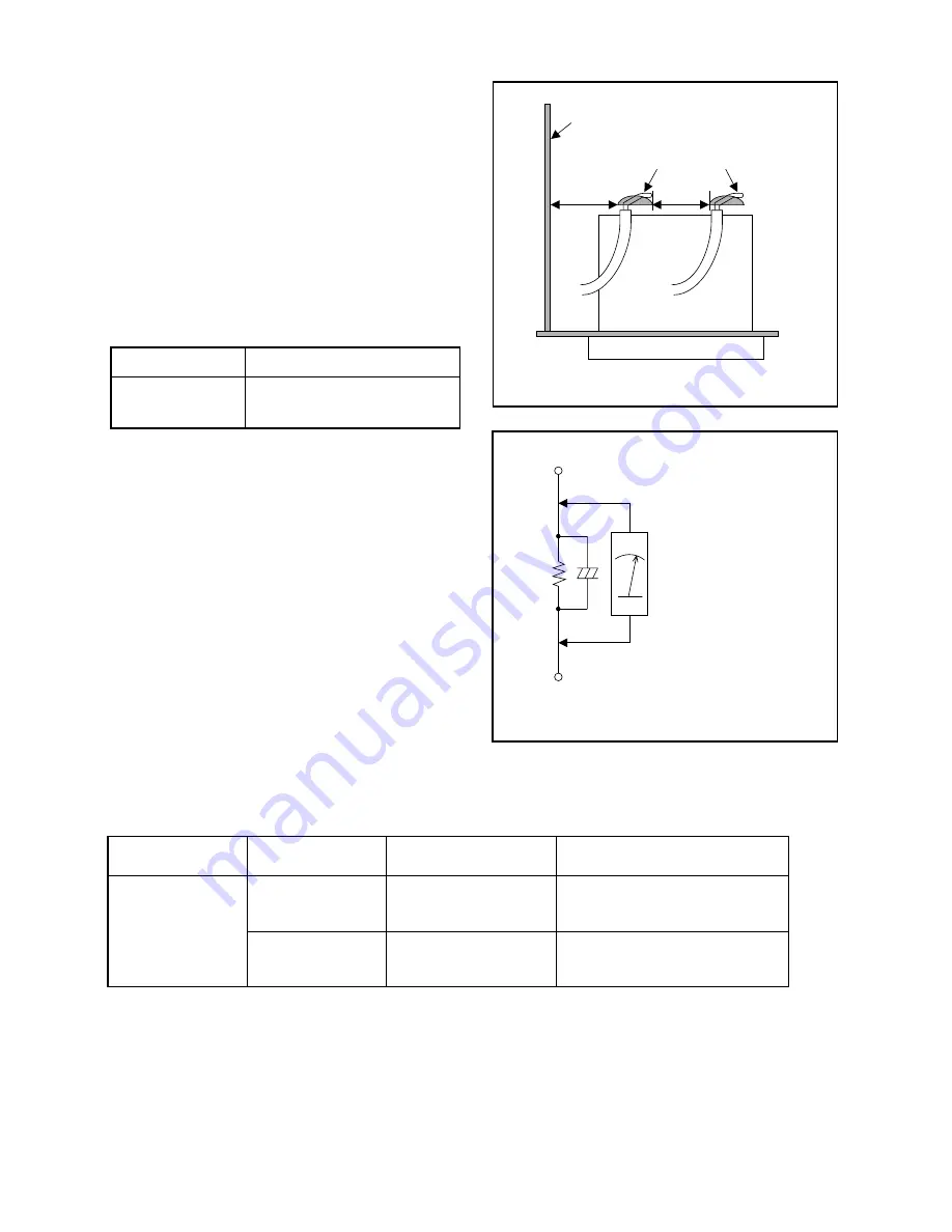
Fig. 1

Chassis or Secondary Conductor

Primary Circuit 

d'

d

AC Voltmeter
(High Impedance)

Exposed Accessible Part

B

One side of 
Power Cord Plug Prongs

Z

Fig. 2

Safety Check after Servicing

Examine the area surrounding the repaired location
for damage or deterioration. Observe that screws,
parts, and wires have been returned to their original
positions. Afterwards, do the following tests and con-
firm the specified values to verify compliance with
safety standards.

1. Clearance Distance

When replacing primary circuit components, confirm
specified clearance distance (d) and (d’) between sol-
dered terminals, and between terminals and surround-
ing metallic parts. (See Fig. 1)

Table 1 : Ratings for selected area

Note:

 This table is unofficial and for reference only. 

Be sure to confirm the precise values.

2. Leakage Current Test

Confirm the specified (or lower) leakage current
between B (earth ground, power cord plug prongs)
and externally exposed accessible parts (RF termi-
nals, antenna terminals, video and audio input and
output terminals, microphone jacks, earphone jacks,
etc.) is lower than or equal to the specified value in the
table below. 

Measuring Method  (Power ON) :

Insert load Z between B (earth ground, power cord
plug prongs) and exposed accessible parts. Use an
AC voltmeter to measure across the terminals of load
Z. See Fig. 2 and the following table.

AC Line Voltage

Clearance Distance (d), (d’)

220 to 240 V


3 mm(d)


6 mm(d’) 

Table 2: Leakage current ratings for selected areas

Note:

 This table is unofficial and for reference only. Be sure to confirm the precise values.

AC Line Voltage

Load Z

Leakage Current (i)

One side of power cord plug 

prongs (B) to:

220 to 240 V

2k

Ω 

RES. 

Connected in 

parallel

i

0.7mA AC Peak

i

2mA DC

RF or

Antenna terminals

50k

 RES. 

Connected in 

parallel

i

0.7mA AC Peak

i

2mA DC

A/V Input, Output

Summary of Contents for D8B-M1000ZB

Page 1: ...n Section I Specifications I Preparation for Servicing I Adjustment Procedures I Schematic Diagrams I CBA s I Exploded views I Parts List When servicing the deck mechanism refer to MK14 Deck Mechanism...

Page 2: ...9 1 Function Indicator Symbols 1 10 1 Block Diagrams 1 11 1 Schematic Diagrams CBA s and Test Points 1 12 1 Waveforms 1 13 1 Wiring Diagram VCR Section 1 14 1 Wiring Diagram DVD Section 1 14 2 IC Pin...

Page 3: ...put R P Vp p 0 8 1 0 1 2 1 3 Video S N Y R P dB 40 45 SP Mode W O Burst 1 4 Video Color S N AM R P dB 37 41 SP Mode 1 5 Video Color S N PM R P dB 30 36 SP Mode 1 6 Resolution PB Line 230 245 SP Mode 2...

Page 4: ...re 5 C 40 C ITEM CONDITIONS UNIT NOMINAL LIMIT 1 Video Output 75 load Vpp 1 0 0 1 2 Optical Digital Out dBm 18 3 Audio PCM 3 1 Output Level 1 kHz 0 dB 47k load Vrms 2 0 3 2 S N 47k load dB 90 3 3 Freq...

Page 5: ...s turned on Do not look directly at the laser beam CAUTION Use of controls and adjustments or doing procedures other than those specified herein may result in hazardous radiation exposure Location Top...

Page 6: ...cal for safety Replace only with part number specified B In addition to safety other parts and assemblies are specified for conformance with regulations applying to spurious radiation These must also...

Page 7: ...2 Leakage Current Test Confirm the specified or lower leakage current between B earth ground power cord plug prongs and externally exposed accessible parts RF termi nals antenna terminals video and a...

Page 8: ...achine then apply hot air to the Flat Pack IC about 5 to 6 seconds Fig S 1 1 2 Remove the flat pack IC with tweezers while apply ing the hot air 3 Bottom of the flat pack IC is fixed with glue to the...

Page 9: ...removing entire flat pack IC first apply soldering iron to center of the flat pack IC and heat up Then remove glue will be melted Fig S 1 6 4 Release the flat pack IC from the CBA using twee zers Fig...

Page 10: ...Installation 1 Using desoldering braid remove the solder from the foil of each pin of the flat pack IC on the CBA so you can install a replacement flat pack IC more easily 2 The I mark on the flat pac...

Page 11: ...ed to remove any static electricity that may be charged on the body 2 Ground for Workbench 1 Be sure to place a conductive sheet or copper plate with proper grounding 1M on the workbench or other surf...

Page 12: ...nto the Deck Mechanism Assembly and press the PLAY button The tape will be loaded into the Deck Mechanism Assembly Make sure the power is on connect TP501 S INH to GND This will stop the function of T...

Page 13: ...ference Notes ID LOC No PART REMOVAL Fig No REMOVE UNHOOK UNLOCK RELEASE UNPLUG DESOLDER Note 1 Top Case D1 8 S 1 2 Front Assembly D2 3 L 1 3 L 2 1 1 1 1 2 3 Top Bracket D2 3 S 2 4 DVD Mechanism Assem...

Page 14: ...Fig D4 2 2 Short the three short lands of FPC cable with sol der before removing the FFC cable CN201 from it If you disconnect the FFC cable CN201 the laser diode of pickup will be destroyed Fig D4 C...

Page 15: ...te 6 Power Supply CBA 7 Loader Holder 4 DVD Mechanism Assembly Fig D3 CN201 CN301 S 7 8 DVD Main CBA Unit DVD Mechanism A Fig D4 S 7 View for A Short the three short lands by soldering Either of two p...

Page 16: ...mbly Fig D6 Desolder Lead with blue stripe From FE Head BOTTOM VIEW Lead connections of Deck Assembly and Main CBA Desolder From Capstan Motor Assembly Printing side Desolder From Cylinder Assembly Fr...

Page 17: ...Mechanism HOW TO EJECT MANUALLY 1 Remove the Top Case Front Assembly and Top Bracket 2 Remove four Screws S 3 in Fig D3 Do not disconnect connectors 3 While lifting up the DVD Mechanism rotate the rou...

Page 18: ...Press STOP to cancel the auto adjustment mode 5 Eject the Alignment Tape FL6A 3 To check reset the initial function setting Preparation 1 Enter the service mode 2 Check the 0 FUNC SET value 1 in Fig...

Page 19: ...unit in that order Fig a appears on the screen 2 Press CLEAR C RESET button on the remote control unit Fig b appears on the screen When OK appears on the screen the factory default will be set 3 To ex...

Page 20: ...again 8 Turn the power on by pressing the STANDBY ON button and the tray will close 9 Press DVD 1 2 3 4 and DISPLAY buttons on the remote control unit in that order Fig g appears on the screen 10 Pres...

Page 21: ...ctly When the drum is not working properly P ON Power safety detection MODE INDICATOR ACTIVE When reel or capstan mechanism is not functioning correctly A R is displayed on a TV screen Refer to Fig 1...

Page 22: ...Q507 SENS INH IC501 SERVO SYSTEM CONTROL 5 6 SENSOR CBA SENSOR CBA END S ST S Q504 Q503 REC SAFETY END S CTL TP503 CTL TO DVD SYSTEM CONTROL SERVO BLOCK DIAGRAM DVD SECTION TO DVD VIDEO AUDIO BLOCK D...

Page 23: ...89 88 87 CHARA INS CCD 1H DELAY SP BYPASS MUTE PB EE IN1 TUNER IN1 TUNER MUTE PB EE FRT IN2 FRT IN2 AGC P R R Y C P R P R P EP Y DELAY Y C MIX 21 79 78 AGC VXO OSD CHARACTER MIX FBC 1 2 58 59 65 29 28...

Page 24: ...2 AUDIO R IN2 AUDIO L IN2 AUDIO R OUT2 AUDIO L OUT2 JACK A CBA AUDIO IN2 5 5 AUDIO OUT2 1 1 CN2017 CN2018 JK101 AUDIO R OUT1 AUDIO L OUT1 2 6 1 3 AUDIO R IN1 AUDIO L IN1 IC751 OUTPUT SELECT 12 13 14 1...

Page 25: ...RECTIFIER 2 4 Q1001 Q1003 Q1008 Q1004 7 8 1 2 3 4 IC1001 ERROR VOLTAGE DET T0011 MAIN CBA POWER SUPPLY CBA HOT CIRCUIT BE CAREFUL 20 19 18 17 16 15 14 13 12 11 2 EV 1 2V 3 EV 1 2V 4 EV 3 3V 5 EV 3 3V...

Page 26: ...TOR M SPINDLE MOTOR IC101 MICRO CONTROLLER SLED MOTOR DRIVE FOCUS ACTUATOR DRIVE SPINDLE MOTOR DRIVE TRACKING ACTUATOR DRIVE 126 TRAY IN SLD 67 SPDL 66 TRACKING DRIVE 127 FOCUS DRIVE 65 TO DIGITAL SIG...

Page 27: ...ROM FLASH ROM FDQ 0 15 FADR 0 19 SDRAM DATA 0 15 PICK UP UNIT TO DVD SYSTEM CONTROL SERVO BLOCK DIAGRAM DVD MAIN CBA UNIT IC503 SDRAM SDRAM DATA 0 15 SDRAM ADDRESS 0 10 2 13 42 53 22 26 29 34 159 178...

Page 28: ...R VIDEO G 3 3 ASPECT TO DIGITAL SIGNAL PROCESS BLOCK DIAGRAM TO DVD SYSTEM CONTROL SERVO BLOCK DIAGRAM VIDEO B ASPECT TO AUDIO BLOCK DIAGRAM VCR SECTION TO SERVO SYSTEM CONTROL BLOCK DIAGRAM VCR SECT...

Page 29: ...itute replacement parts that do not have the same safety characteristics as specified in the parts list may create shock fire or other hazards Notes 1 Do not use the part number shown on these draw in...

Page 30: ...acement parts which are listed with their part numbers in the parts list section of the service manual 4 Voltage indications for PLAY and REC modes on the schematics are as shown below 5 How to read c...

Page 31: ...1 12 3 E8GA1SCM1 Main 1 8 Schematic Diagram VCR Section Comparison Chart of Models and Marks MODEL MARK D8B M1000ZB A D8C M1000DB B...

Page 32: ...1 12 4 E8GA1SCM2 Main 2 8 Sensor Schematic Diagram VCR Section Comparison Chart of Models and Marks MODEL MARK D8B M1000ZB A D8C M1000DB B...

Page 33: ...1 12 5 E8GA1SCM3 Main 3 8 Schematic Diagram VCR Section Comparison Chart of Models and Marks MODEL MARK D8B M1000ZB A D8C M1000DB B...

Page 34: ...1 12 6 E8GA1SCM4 Main 4 8 Schematic Diagram VCR Section...

Page 35: ...1 12 7 E8GA1SCM5 Main 5 8 Schematic Diagram VCR Section...

Page 36: ...1 12 8 E8GA1SCM6 Main 6 8 Schematic Diagram VCR Section...

Page 37: ...1 12 9 E8GA1SCM7 Main 7 8 DVD Open Close Schematic Diagram VCR Section...

Page 38: ...1 12 10 E8GA2SCM8 Main 8 8 Schematic Diagram B VCR Section Comparison Chart of Models and Marks MODEL MARK D8B M1000ZB A D8C M1000DB B...

Page 39: ...check to see that all components in the power supply circuit are not defective before you connect the AC plug to the AC power supply Otherwise it may cause some components in the power supply circuit...

Page 40: ...1 12 12 E8GA1SCJ Jack A Schematic Diagram VCR Section...

Page 41: ...1 12 13 E8GA1SCD1 DVD Main 1 3 Schematic Diagram DVD Section 1 NOTE Either IC461 or IC462 is used for DVD MAIN CBA UNIT...

Page 42: ...1 12 14 E8GA1SCD2 DVD Main 2 3 Schematic Diagram DVD Section Comparison Chart of Models and Marks MODEL MARK D8B M1000ZB A D8C M1000DB B...

Page 43: ...1 12 15 E8GA1SCD3 DVD Main 3 3 Schematic Diagram DVD Section...

Page 44: ...1 12 16 Sensor CBA Top View END S TP502 RF SW TP504 WF1 S INH TP501 V OUT TP751 WF3 C PB TP301 WF2 Main CBA Top View BE8G00F01012A BHF300F01012A BHF300F01012B...

Page 45: ...1 12 17 PIN12OF CN1601 WF5 PIN 10 OF CN1601 WF4 PIN 8 OF CN1601 WF8 PIN 14 OF CN1601 WF6 PIN 6 OF IC1403 WF9 PIN 16 OF CN1601 WF7 Main CBA Bottom View BE8G00F01012A...

Page 46: ...1 12 18 DVD Open Close CBA Top View DVD Open Close CBA Bottom View Jack A CBA Top View Jack A CBA Bottom View BE8G00F01012C BE8G00F01021C...

Page 47: ...selectable power supply circuit is used in this unit If Main Fuse F1001 is blown check to see that all components in the power supply circuit are not defective before you connect the AC plug to the A...

Page 48: ...IO L 1V 0 5ms WF8 WF9 SPDIF 1V 0 1 s Pin 8 of CN1601 Pin 10 of CN1601 Pin 12 of CN1601 Pin 14 of CN1601 Pin 16 of CN1601 NOTE Input COLOR BAR SIGNAL WITH 1KHz AUDIO SIGNAL DVD AUDIO R 1V 0 5ms V OUT E...

Page 49: ...008 EV 3 3V 1 1 DVD OPEN CLOSE 2 2 CN502 CN051 CN051A CL051A CL052A JW002 JW003 JW004 CL051B CL052B POWER SUPPLY CBA JUNCTION CBA 1 AL 44V 2 GND 3 AL 12V 4 GND 5 AL 5V 5 AL 5V 6 GND 7 AL 20 5V 8 GND 9...

Page 50: ...PD PD MONI DVD LD VREF NU GND B DVD P ON 5V CD DVD D A C NU GND LD DETECTOR FS TS 7 9 11 2 3 6 5 4 CN601 VIDEO Y 1 I P SW NU 2 ASPECT 3 VODEO R 4 GND 5 GND 7 GND 9 GND 11 GND 15 VIDEO B 6 VIDEO G 8 VI...

Page 51: ...or L 15 OUT C ROTA Color Phase Rotary Changeover SIgnal H L 16 OUT H A SW Video Head Amp Switching Pulse H L 17 IN H A COMP Head Amp Comparator Signal H L 18 OUT RF SW Video Head Switching Pulse H L 1...

Page 52: ...Pin Level by using 8POUT 1 and 8POUT 2 Hi z L Pin No Mark IN OUT Signal Name Function Active Level 61 A NU Not Used B IN SECAM H SECAM Mode at High H L 62 OUT AUDIO SW1 Audio IN OUT Control Signal H L...

Page 53: ...etection Pulse PULSE 88 NU Not Used 89 NU Not Used 90 IN D PFG Drum Motor Phase Frequency Generator PULSE 91 AMPVREF OUT V Ref for CTL AMP 92 AMPVREF in V Ref for CTL AMP 93 P80 C P80 C Terminal 94 IN...

Page 54: ...52BCSJX_NL CD4052BNSR CD4053BCSJX_NL CD4053BNSR TC4052BF ELNF TC4053BF EL N F 1 MID 32A22F PT204 6B 12 E C 5 4 8 1 BR24L02F WE2 CAT24WC02WI TE13 B1 E B2 C1 C2 FMG4A T148 RN1511 TE85R F KRC103S RTK P K...

Page 55: ...DVD Open Close CBA JW008 JW003 JW006 JW007 JW002 JW001 2L091 2L012 2L054 2B55 B Main CBA JW004 Power Supply CBA These FFC cables are included in 1B2 DVD mechanism Junction CBA 2L021 F1001 A B A A3 A7...

Page 56: ...8GA1PEX Packing S1 A14 X4 Unit S3 S2 S2 S2 Some Ref Numbers are not in sequence X2 X3 X1 X34 X35 S9 A Comparison Chart of Models and Marks Model Mark D8B M1000ZB D8C M1000DB A B A X20A X20B X20C X20 A...

Page 57: ...VM424064 2B54 PLATE GROUND RCA H9700ED 0VM306867 2B55 PLATE GROUND 21P H9700ED 0VM416444 2L011 SCREW P TIGHT M3X8 BIND HEAD GBJP3080 2L012 SCREW S TIGHT M3X6 BIND HEAD GBJS3060 2L020 SCREW P TIGHT M3X...

Page 58: ...ASDL471 C126 ELECTROLYTIC CAP 470 F 6 3V M CE0KMASDL471 C127 ELECTROLYTIC CAP 10 F 16V M CE1CMASDL100 C128 ELECTROLYTIC CAP 22 F 6 3V M H7 CE0KMASSL220 C133 CHIP CERAMIC CAP 1608 F Z 0 1 F 50V or CHD1...

Page 59: ...FZ104 C370 B CERAMIC CAP AX Y M 0 01 F 16V CCA1CMT0Y103 Ref No Mark Description Part No C371 B CHIP CERAMIC CAP 1608 B K 0 022 F 50V or CHD1JK30B223 B CHIP CERAMIC CAP 1608 B K 0 022 F 25V CHD1EK30B22...

Page 60: ...F 6 3V H7 CE0KMAVSL101 C553 ELECTROLYTIC CAP 22 F 10V M H7 CE1AMAVSL220 Ref No Mark Description Part No C555 CHIP CERAMIC CAP 1608 B K 0 1 F 25V or CHD1EK30B104 CHIP CERAMIC CAP 1608 B K 0 1 F 16V CHD...

Page 61: ...18 ZENER DIODE MTZJT 7711A or QDTA00MTZJ11 Ref No Mark Description Part No DIODE ZENER 11BSA T26 or NDTA011BST26 ZENER DIODE DZ 11BSAT265 NDTA00DZ11BS D119 ZENER DIODE MTZJT 7711A or QDTA00MTZJ11 DIOD...

Page 62: ...ription Part No Q506 PHOTO TRANSISTOR PT204 6B 12 or NPWZT2046B12 PHOTO TRANSISTOR MID 32A22F NPWZ1D32A22F Q507 TRANSISTOR KTC3199 Y AT P or NQSYKTC3199P TRANSISTOR KTC3199 GR AT P NQS4KTC3199P Q508 T...

Page 63: ...J 470 RRXA471YF002 R322 CHIP RES 1 10W J 10k or RRXAJR5Z0103 Ref No Mark Description Part No RES CHIP 1608 1 10W J 10k RRXA103YF002 R323 CHIP RES 1 10W J 1 2k or RRXAJR5Z0122 RES CHIP 1608 1 10W J 1...

Page 64: ...1 10W J 3 9k RRXA392YF002 R534 CARBON RES 1 6W J 330 or RCX6JATZ0331 Ref No Mark Description Part No CARBON RES 1 4W J 330 RCX4JATZ0331 R535 CHIP RES 1 10W J 3 9k or RRXAJR5Z0392 RES CHIP 1608 1 10W...

Page 65: ...02 R1210 CHIP RES 1 10W F 30k or RRXAFR5H3002 CHIP RES 1608 1 10W F 30k or RRXAFR5Z3002 Ref No Mark Description Part No RES CHIP 1608 1 10W F 30 0k RTW3002YF002 R1211 CHIP RES 1 10W J 1k or RRXAJR5Z01...

Page 66: ...4B or SST0101HH013 TACT SWITCH SKQSAF001A or SST0101AL041 TACT SWITCH TC 1104 H 9 5 SST0101DNG01 SW2021 TACT SWITCH KSM0614B or SST0101HH013 TACT SWITCH SKQSAF001A or SST0101AL041 TACT SWITCH TC 1104...

Page 67: ...1N4005 NDWZ001N4005 D1004 RECTIFIER DIODE 1N4005 or NDQZ001N4005 DIODE RECTIFIER 1N4005 or NDLZ01N4005S RECTIFIER DIODE 1N4005 NDWZ001N4005 D1006 SWITCHING DIODE 1SS133 T 77 or QDTZ001SS133 DIODE SWIT...

Page 68: ...L0A0280 005 WAE0172LTE06 F1001 FUSE T1 6AL 250V or PAGC20BW3162 FUSE 50T016H 1 6A 250V PAGH20BHV162 FH1001 FUSE HOLDER MSF 015 LF B110 or XH01Z00LY002 FUSE HOLDER DFH 001 XH01Z00RP001 FH1002 FUSE HOLD...

Page 69: ...S 1 10W J 75 or RRXAJR5Z0750 RES CHIP 1608 1 10W J 75 RRXA750YF002 MISCELLANEOUS JK1402 RGB CONNECTOR MRC 021V 03 ABS B11 JXGL210LY006 JW003 FLAT CABLE 10P AWG26 2651 P2 0 190 WX3810S6FF19 JW004 FLAT...

Page 70: ...D8B M1000ZB D8C M1000DB E8GA1BD 2FD 2007 05 14...

Reviews: