background image

2-4-4

H9500DA

[1]

(S-1)

(S-1)

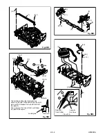
Fig. DM3

Fig. DM4

Locking tab

View for A

First, while pushing the locking tab as 
shown in the right, slide and pull up the right 
side on [2] to release Pin A and Pin B from 
the slots A.
Then, remove Pin C and Pin D on [2] from 
the slots B as shown.

[2]

Pin A

Slots B

Pin C

Pin B

Pin D

Pull up

Slide

Slot A

Slot A

1

2

A

(L-12)

[49]

[50]

[7]

(S-2)

A

Fig. DM6

View for A

Desolder
from bottom

Lead with 
Red Stripe

[3]

[4]

[5]

[6]

(L-1)

(L-2)

(P-1)

Fig. DM5

(L-3)

(S-1A)

Summary of Contents for DPVR-4604

Page 1: ...I Schematic Diagrams I CBA s Sec 2 Deck Mechanism Section I Standard Maintenance I Alignment for Mechanism I Disassembly Assembly of Mechanism I Alignment Procedures of Mechanism Sec 3 Exploded views...

Page 2: ...lectrical Adjustment Instructions 1 7 1 FIRMWARE Renewal Mode 1 8 1 Block Diagrams 1 9 1 Schematic Diagrams CBA s and Test Points 1 10 1 Waveforms 1 11 1 Wiring Diagrams 1 12 1 IC Pin Function Descrip...

Page 3: ...de W O Burst 1 4 Video Color S N AM R P dB 37 41 SP Mode 1 5 Video Color S N PM R P dB 30 36 SP Mode 1 6 Resolution PB Line 230 245 SP Mode 2 Servo 2 1 Jitter Low sec 0 07 0 12 SP Mode 2 2 Wow Flutter...

Page 4: ...3 Load imp 100 K ohm 4 Room ambient 5 C 40 C ITEM CONDITIONS UNIT NOMINAL LIMIT 1 Video Output 75 ohm load Vpp 1 0 0 1 2 Optical Digital Out dBm 18 3 Audio PCM 3 1 Output Level 1kHz 0dB Vrms 2 0 3 2 S...

Page 5: ...eyes at least 30cm away from the pickup lens when the diode is turned on Do not look directly at the laser beam Caution Use of controls and adjustments or doing procedures other than those specified h...

Page 6: ...e especially 1 Wires covered with PVC tubing 2 Double insulated wires 3 High voltage leads D Use specified insulating materials for hazardous live parts Note especially 1 Insulation tape 2 PVC tubing...

Page 7: ...2 Leakage Current Test Confirm the specified or lower leakage current between B earth ground power cord plug prongs and externally exposed accessible parts RF termi nals antenna terminals video and a...

Page 8: ...e the flat pack IC with tweezers while apply ing the hot air 3 Bottom of the flat pack IC is fixed with glue to the CBA when removing entire flat pack IC first apply soldering iron to center of the fl...

Page 9: ...pins of the flat pack IC you can remove it easily Fig S 1 3 2 Affix the wire to a workbench or solid mounting point as shown in Fig S 1 5 3 While heating the pins using a fine tip soldering iron or h...

Page 10: ...cur due to a potential difference caused by electro static charge during unpacking or repair work 1 Ground for Human Body Be sure to wear a grounding band 1M that is prop erly grounded to remove any s...

Page 11: ...e Deck Mechanism Assembly and press the PLAY button The tape will be loaded into the Deck Mechanism Assembly Make sure the power is on connect TP501 SENSOR INHIBITION to GND This will stop the functio...

Page 12: ...LUG DESOLDER Note 1 Top Cover D1 7 S 1 2 Front Assembly D2 S 2 7 L 1 1 1 1 1 2 3 Top Bracket D2 2 S 3 2 S 3A 4 DVD Mecha Assembly D3 3 S 4 CN302 CN401 CN601 5 DVD Main CBA D4 2 S 5 CN201 CN301 2 2 1 2...

Page 13: ...ng the FFC cable CN301 from it If you disconnect the FFC cable CN301 the laser diode of pickup will be destroyed Fig D4 2 3 Disconnect Connector CN201 Remove two Screws S 5 and lift the DVD Main CBA F...

Page 14: ...C Short the three short lands by soldering FPC Cable Slide View for C S 5 CN201 5 DVD Main CBA Unit DVD Mecha S 5 CN301 Fig D4 S 7 S 6 S 7 6 Rear Unit S 7 CN003 Fig D5 9 Rear Panel 7 Power Supply CBA...

Page 15: ...ain CBA 11 Deck Assembly 12 Main CBA SW507 LD SW Pin BOTTOM VIEW Lead connections of Deck Assembly and Main CBA Desolder Desolder Lead with blue stripe Lead with blue stripe Desolder Desolder From FE...

Page 16: ...3 17 Deck Pedestal Fig D9 DVD Mecha Deck Assembly Tray Top Cover 3 2 Rotate this roulette in the direction of the arrow 1 2 To Remove the Disc Manually 1 Remove the Top Cover 2 Rotate this roulette in...

Page 17: ...e Dual trace with 10 1 probe V Range 0 001 50V Div F Range DC AC 20MHz 2 Alignment Tape FL6A Head Switching Position Adjustment Purpose To determine the Head Switching point during playback Symptom of...

Page 18: ...t Then plug it again 7 Turn the power on by pressing the power button and the tray will close 8 Press 1 2 3 4 and DISPLAY buttons on the remote control unit in that order Fig g appears on the screen 9...

Page 19: ...1 4 4 POWER LED KEY SWITCH CL505 D591 CL591 AL 5V FUNCTION CBA SDA SCL IC502 MEMORY 72 32 19 83 IIC BUS SCL D V SYNC D REC H INPUT SELECT RF SW H A SW C ROTA IIC BUS SDA H A COMP V ENV 58 C SYNC C SYN...

Page 20: ...95 94 93 90 89 88 87 CHARA INS CCD 1H DELAY SP BYPASS MUTE PB EE IN1 TUNER IN1 TUNER MUTE PB EE FRT IN2 FRT IN2 AGC P R R Y C P R P R P EP Y DELAY Y C MIX 79 78 AGC VXO OSD CHARACTER MIX FBC 1 2 65 69...

Page 21: ...PB ON SP LP ON P TUNER IN2 IN1 R ALC DET ALC IC301 AUDIO SIGNAL PROCESS 15 13 17 4 A PB REC CL504 3 A COM 1 AE H 2 AE H FE H A PB REC 4 A COM 3 AE H 1 AE H FE H 2 CL287 AUDIO HEAD AUDIO ERASE HEAD ACE...

Page 22: ...BA Hi Fi A R 7 Hi Fi COM 8 Hi Fi A L 9 CL251 IC451 MTS SAP Hi Fi AUDIO PROCESS Hi Fi HEAD AMP REC AUDIO SIGNAL PB AUDIO SIGNAL Mode SP REC DVD AUDIO SIGNAL AFV CBA JK101 A OUT1 R A OUT1 L 2 6 2 6 1 3...

Page 23: ...01 ERROR VOLTAGE DET T001 MAIN CBA POWER SUPPLY CBA Q1009 VOLTAGE DETECTION REG HOT CIRCUIT BE CAREFUL 20 19 18 17 16 15 14 13 12 11 1 EV 1 5V 2 EV 1 5V 3 EV 1 5V 4 EV 3 3V 5 EV 3 3V 13 P ON 5V 14 EV...

Page 24: ...LL X TAL OSC 36 864MHz OSC SPINDLE MOTOR DRIVE TRACKING ACTUATOR DRIVE EXT CLOCK CLK33M BE CLOCK 172 170 150 TRAY OUT TRAY IN FG IN 97 SLD 70 SPDL 71 TRACKING DRIVE 152 FOCUS DRIVE 60 66 TO DVD VIDEO...

Page 25: ...OLLER TIMER WATCH DOG TIMER 32BIT CPU STREAM I F EXTERNAL MEMORY I F SDRAM ECC UMAC 124 125 122 123 128 129 126 127 131 130 135 133 132 134 78 DEBUG BCU INST CACHE D TYPE LATCH DATA CACHE D A D A D A...

Page 26: ...DVD A L DVD A R PCM BCK SPDIF PCM DATA0 PCM LRCLK ADAC MD ADAC MC ADAC ML PCM SCLK MAIN CBA DVD MAIN CBA UNIT DVD AUDIO SIGNAL DATA AUDIO SIGNAL 18 18 SPDIF A MUTE 3 3V Q1204 WF9 3 WF7 WF8 CN601 1 1 V...

Page 27: ...itute replacement parts that do not have the same safety characteristics as speci fied in the parts list may create shock fire or other hazards Notes 1 Do not use the part number shown on these draw i...

Page 28: ...n the parts list section of the service manual 4 Wire Connectors 1 Prefix symbol CN means connector can disconnect and reconnect 2 Prefix symbol CL means wire solder holes of the PCB wire is soldered...

Page 29: ...Main 1 10 Schematic Diagram VCR Section 1 10 3 1 10 4 H95B0SCM1...

Page 30: ...Main 2 10 Sensor Schematic Diagram VCR Section 1 10 5 1 10 6 H95B0SCM2 Note When it is necessary to replace one or more of the following Diodes all one should be replaced D501 D502 D503 D504 1...

Page 31: ...1 10 7 1 10 8 H95B0SCM3 Main 3 10 Schematic Diagram VCR Section...

Page 32: ...Main 4 10 Schematic Diagram VCR Section 1 10 9 1 10 10 H95B0SCM4...

Page 33: ...Main 5 10 Schematic Diagram VCR Section 1 10 11 1 10 12 H95B0SCM5...

Page 34: ...Main 6 10 Schematic Diagram VCR Section 1 10 13 1 10 14 H95B0SCM6...

Page 35: ...Main 7 10 Schematic Diagram VCR Section 1 10 15 1 10 16 H95B0SCM7...

Page 36: ...Main 8 10 DVD Open Close Schematic Diagram VCR Section 1 10 17 1 10 18 H95B0SCM8...

Page 37: ...1 10 19 1 10 20 Main 9 10 Schematic Diagram VCR Section H95B0SCM9...

Page 38: ...Main 10 10 Schematic Diagram VCR Section 1 10 21 1 10 22 H95B0SCM10...

Page 39: ...tection against fire hazard replace only with the same type fuse CAUTION Fixed voltage or Auto voltage selectable power supply circuit is used in this unit If Main Fuse F1001 is blown check to see tha...

Page 40: ...1 10 25 1 10 26 Jack Schematic Diagram VCR Section H95B0SCJ...

Page 41: ...1 10 27 1 10 28 Function Schematic Diagram VCR Section H95B0SCF...

Page 42: ...1 10 29 1 10 30 AFV Schematic Diagram VCR Section H95B0SCAFV...

Page 43: ...Main CBA Top View Sensor CBA Top View SW P VR501 CTL TP503 V OUT TP751 WF3 C PB TP301 WF2 RF SW TP504 WF1 S INH TP501 1 10 31 BH9510F01014A BHB300F01014 A BHB300F01014 B 1 10 32 Sensor CBA Top View...

Page 44: ...1 10 33 Main CBA Bottom View BH9510F01014A 1 10 34...

Page 45: ...1 10 35 Function CBA Top View BH9510F01014B 1 10 36 Function CBA Bottom View BH9510F01014C DVD OPEN CLOSE CBA Top View DVD OPEN CLOSE CBA Bottom View...

Page 46: ...A VARIABLE ISOLATION TRANSFORMER IS REQUIRED CAUTION Fixed voltage or Auto voltage selectable power supply circuit is used in this unit If Main Fuse F1001 is blown check to see that all components in...

Page 47: ...1 10 39 1 10 40 Jack CBA Top View Jack CBA Bottom View AFV CBA Top View AFV CBA Bottom View BHC400F01091 BH9510F01022C...

Page 48: ...DVD Main 1 3 Schematic Diagram DVD Section H95B0SCD1 1 10 41 1 10 42...

Page 49: ...1 10 43 1 10 44 DVD Main 2 3 Schematic Diagram DVD Section H95B0SCD2...

Page 50: ...3 4 0 1 127 2 0 2 0 32 64 0 8 0 8 96 3 4 3 4 128 2 0 2 0 PIN NO PLAY STOP PIN NO PLAY STOP PIN NO PLAY STOP PIN NO PLAY STOP 129 2 0 2 0 161 0 5 0 5 193 225 1 9 1 9 130 2 2 2 2 162 1 4 1 4 194 0 0 22...

Page 51: ...DVD Main 3 3 Schematic Diagram DVD Section 1 10 47 H95B0SCD3 1 10 48...

Page 52: ...T E E 10usec 50mV x 10 WF3 TP751 of Main CBA WF3 UPPER WF1 LOWER V OUT 0 1V x 10 RF SW 0 5V x 10 50usec TP751 of Main CBA TP504 of Main CBA WF2 C PB 10mV x 10 RF SW 0 5V x 10 5msec UPPER LOWER WF1 TP5...

Page 53: ...IC1402 WF5 Pin 9 of CN1601 VIDEO Y 0 2V 20 sec VIDEO C 0 2V 20 sec VIDEO CVBS 0 5V 20 sec WF7 AUDIO L Pin 13 of CN1601 1V 0 5msec WF8 AUDIO R Pin 15 of CN1601 1V WF9 SPDIF Pin 18 of CN1601 1V 0 1 sec...

Page 54: ...CN1601 EV 1 5V EV 1 5V EV 3 3V EV 1 5V EV 3 3V GND GND GND GND GND GND GND EV 9V P ON 5V EV 9V FP STB P ON 3 3V FP DIN PWRCON OUT SEL REMOTE DVD FP CLK VIDEO R VIDEO Y ASPECT VIDEO B GND GND VIDEO G...

Page 55: ...3 4 TRAY OUT TRAY IN GND 5 6 SP 7 SP 8 SL 9 SL FG IN P ON 3 3V D TRAY IN DRIVE CBA FG CBA FG SENSOR TRAY OUT M SLED MOTOR M SPINDLE MOTOR EV 1 5V EV 1 5V EV 3 3V EV 1 5V EV 3 3V GND GND GND GND GND 1...

Page 56: ...L 19 OUT Hi Fi H SW HiFi Audio Head Switching Pulse H L 20 IN DAVN L VPS PDC Data Receive L L 21 OUT DVD POWER DVD Power Control Signal H 22 NU Not Used 23 OUT POWER LED POWER LED Signal Output H L 2...

Page 57: ...tor Control Signal PWM 77 OUT D CONT Drum Motor Control Signal PWM 78 OUT C F R Capstan Motor FWD REV Control Signal FWD L REV H H L 79 IN S REEL Supply Reel Rotation Signal PULSE 80 IN T REEL Take Up...

Page 58: ...ta 1 Input 4 In K2 Key Data 2 Input 5 VSS GND 6 VDD Power Supply 7 Out a Segment Output 8 b 9 c 10 d 11 e 12 f 13 g 14 h 15 VEE Pull Down Level 16 Out i Segment Output 17 Out 7G Grid Output 18 6G 19 5...

Page 59: ...020 Y 2SC3266 Y TPE2 KTA1281 Y KTC3205 Y E C B A K C E LTV 817 B C F EL817 A B C G D S 2SK3566 1 4 8 5 NJM4558D KIA4558P 1 2 3 4 PQ070XF01SZ 81 80 31 100 50 30 1 51 QSZAC0RMB159 LA71750EM MPB E 16 9 8...

Page 60: ...rvice Fixtures and Tools 2 2 1 Mechanical Alignment Procedures 2 3 1 Disassembly Assembly Procedures of Deck Mechanism 2 4 1 Alignment Procedures of Mechanism 2 4 8 Sec 2 Deck Mechanism Section I Stan...

Page 61: ...3 Recording model only B86 Not used in 2 head model H Hours Check I Change Deck Periodic Service Schedule Ref No Part Name 1 000 H 2 000 H 3 000 H 4 000 H B2 Cylinder Assembly I I B3 Loading Motor Ass...

Page 62: ...hard material but since it is very thin avoid cleaning it vertically 2 Wait for the cleaned part to dry thoroughly before operating the unit 3 Do not reuse a stained head cleaning stick or a stained...

Page 63: ...ignment Tape FL6N8 1 speed only FL6NS8 2 speed only Azimuth and X Value Adjustment of Audio Control Head Adjustment of Envelope Waveform J 2 Guide Roller Adj Screwdriver Available Locally Guide Roller...

Page 64: ...re that the Moving guide preparations are in the Eject Position 4 Turn the LDG Belt in the appropriate direction shown in Fig M1 until the Moving guide prepara tions come to the Eject Position Stop tu...

Page 65: ...the X value and envelope Not good Do the final tape traveling test to see that the tape runs normally in play mode with out creasing or slacking Completion Not good OK OK OK Not good Not good OK Flowc...

Page 66: ...ition of the Audio Control Erase Head Symptom of Misalignment If the Horizontal Position of the Audio Control Erase Head is not properly aligned maximum envelope can not be obtained at the Neutral pos...

Page 67: ...f Guide Roller 2 Refer to Fig M3 so that the waveform looks like the one shown in Fig M9 4 If the envelope is as shown in Fig M8 adjust the height of Guide Roller 3 Refer to Fig M3 so that the wavefor...

Page 68: ...DM6 Desolder 3 S 2 8 8 Loading Motor Assembly T DM1 DM7 Desolder LDG Belt 2 S 3 9 9 AC Head Assembly T DM1 DM7 S 4 10 2 Tape Guide Arm Assembly T DM1 DM8 P 2 11 10 C Door Opener T DM1 DM8 L 4 12 11 Pi...

Page 69: ...ication 34 26 Loading Arm SP Assembly B DM2 DM14 Refer to Alignment Sec Pg 2 4 8 35 34 Loading Arm TU Assembly B DM2 DM14 Refer to Alignment Sec Pg 2 4 8 36 16 26 M Brake TU Assembly HI T DM1 DM15 37...

Page 70: ...2 4 3 H9500DA 14 13 11 10 12 7 49 8 32 43 41 40 31 42 45 44 46 9 36 15 38 37 Fig DM1 Top View 34 19 35 25 26 24 23 27 33 20 28 22 Fig DM2 Bottom View...

Page 71: ...ide and pull up the right side on 2 to release Pin A and Pin B from the slots A Then remove Pin C and Pin D on 2 from the slots B as shown 2 Pin A Slots B Pin C Pin B Pin D Pull up Slide Slot A Slot A...

Page 72: ...Stripe A 8 9 S 4 S 3 LDG Belt Fig DM8 11 13 12 A 10 L 4 Adj Screw P 3 P 2 27 When reassembling 10 and 12 confirm that pin of 10 and pin of 12 are in the groove of 27 as shown Pin of 12 Pin of 10 Groo...

Page 73: ...ig DM13 Align 26 and 27 as shown Bottom View 27 Pin of 36 Pin of 33 Position of Mode Lever when installed Pin of 37 26 When reassembling 27 meet the first groove on 27 to the first tooth on 44 as show...

Page 74: ...2 4 7 H9500DA Refer to the Alignment Section Page 2 4 8 Fig DM14 33 32 L 9 P 5 34 35 Fig DM15 37 39 turn turn 42 43 38 P 6 turn 36 L 10 40 41 C 6 C 7 Fig DM16 44 45 46 L 11 47 48 Slide Fig DM17...

Page 75: ...echanical or electrical parts Alignment points in Eject Position Alignment 1 Loading Arm SP and TU Assembly Install Loading Arm SP and TU Assembly so that their triangle marks point to each other as s...

Page 76: ...DVD PLAYER VIDEO CASSETTE RECORDER DPVR 4604 TABLE OF CONTENTS Exploded Views 3 1 1 Mechanical Parts List 3 2 1 Electrical Parts List 3 3 1 Deck Parts List 3 4 1 Sec 3 Exploded views and Parts List S...

Page 77: ...L033 Function CBA 2L054 2L054 2L091 2L012 2B11 Main CBA A B C DVD Main CBA Unit See Electrical Parts List for parts with this mark Some Ref Numbers are not in sequence 2B15 2B15 2B46 JW001 JW002 JW003...

Page 78: ...3 1 3 H95B0PEX S1 A14 X20 Some Ref Numbers are not in sequence X2 X3 X4 X1 Unit S3 S2 S2 X5 S7 Packing...

Page 79: ...Chassis Assembly Bottom View Lubricating Point B2 B35 B410 B411 B494 B567 L1053 B74 B10 L1191 B73 B9 B12 B492 B11 B571 B37 B126 L1466 B501 B8 B121 L1450 L1450 L1051 L1467 B553 B86 Mark Description Fl...

Page 80: ...B565 L1151 B525 B592 B31 L1406 B148 B521 B590 B487 B573 B574 B499 B587 B508 B558 B557 B3 B417 B584 B591 Mark Description Floil G 684G or Multemp MH D Blue grease SLIDUS OIL 150 B522 B414 B416 B518 B5...

Page 81: ...B563 B300 B562 B482 L1341 B355 B354 B483 B425 L1321 B347 L1321 B361 B359 B529 B360 B514 B313 Some Ref Numbers are not in sequence Mark Description Floil G 684G or Multemp MH D Blue grease SLIDUS OIL 1...

Page 82: ...OR H9500ED 0VM306050 2L011 SCREW S TIGHT M3X8 BIND CHROME GBMS3080 2L012 SCREW S TIGHT M3X8 BIND CHROME GBMS3080 2L021 SCREW S TIGHT M3X26 H9400UD 0VM414507 2L031 SCREW S TIGHT M3X5 BIND HEAD GBMS3050...

Page 83: ...D1JJ3CH471 CHIP CERAMIC CAP CG J 470pF 50V CHD1JJ3CG471 C113 CHIP CERAMIC CAP F Z 0 1 F 50V or CHD1JZ30F104 CHIP CERAMIC CAP F Z 0 1 F 25V or CHD1EZ30F104 CHIP CERAMIC CAP FZ Z 0 1 F 50V CHD1JZ3FZ104...

Page 84: ...820pF 50V or CHD1JJ3CH821 CHIP CERAMIC CAP CH J 820pF 25V or CHD1EJ3CH821 Ref No Description Part No CHIP CERAMIC CAP CG J 820pF 50V CHD1JJ3CG821 C408 CHIP CERAMIC CAP B K 1800pF 50V CHD1JK30B182 C40...

Page 85: ...P CERAMIC CAP CH J 22pF 50V or CHD1JJ3CH220 CHIP CERAMIC CAP CG J 22pF 50V CHD1JJ3CG220 Ref No Description Part No C544 CHIP CERAMIC CAP CH J 22pF 50V or CHD1JJ3CH220 CHIP CERAMIC CAP CG J 22pF 50V CH...

Page 86: ...V M or CE1JMASDL1R0 ELECTROLYTIC CAP 1 F 50V M CE1JMASTL1R0 C1481 ELECTROLYTIC CAP 1 F 50V M or CE1JMASDL1R0 ELECTROLYTIC CAP 1 F 50V M CE1JMASTL1R0 C1482 ELECTROLYTIC CAP 470 F 6 3V M or CE0KMASDL471...

Page 87: ...DVD 6CH MM1567AJBE QSZBA0TMM082 IC1404 IC SWITCH TC4053BF N or QSMBA0STS002 IC SWITCH BU4053BCF E2 QSMDA0TRM010 Ref No Description Part No COILS L052 CHOKE COIL 47 H K or LLBD00PKV007 CHOKE COIL 47 H...

Page 88: ...KTC3199 TRANSISTOR KTC3199 GR or NQS10KTC3199 TRANSISTOR 2SC2785 J or QQSJ02SC2785 Ref No Description Part No TRANSISTOR 2SC2785 H or QQSH02SC2785 TRANSISTOR 2SC2785 F or QQSF02SC2785 TRANSISTOR 2SC18...

Page 89: ...n Part No R150 CHIP RES 1608 1 10W J 47k RRXAJR5Z0473 R251 CHIP RES 1608 1 10W J 39k RRXAJR5Z0393 R252 CHIP RES 1608 1 10W J 2 2k RRXAJR5Z0222 R301 CHIP RES 1608 1 10W J 1 2k RRXAJR5Z0122 R303 CHIP RE...

Page 90: ...J 3 9k RRXAJR5Z0392 R532 CARBON RES 1 4W J 270 RCX4JATZ0271 Ref No Description Part No R533 CHIP RES 1608 1 10W J 3 9k RRXAJR5Z0392 R534 CARBON RES 1 6W J 330 or RCX6JATZ0331 CARBON RES 1 4W J 330 RC...

Page 91: ...RXAJR5Z0222 R1239 CHIP RES 1608 1 10W J 100k RRXAJR5Z0104 R1240 CHIP RES 1608 1 10W J 100k RRXAJR5Z0104 R1245 CHIP RES 1608 1 10W J 10 RRXAJR5Z0100 Ref No Description Part No R1352 CHIP RES 1608 1 10W...

Page 92: ...R5Z0152 R593 CHIP RES 1608 1 10W J 2 2k RRXAJR5Z0222 R594 CHIP RES 1608 1 10W J 3 9k RRXAJR5Z0392 SWITCHES SW591 TACT SWITCH KSM0614B or SST0101HH013 TACT SWITCH SKQSAF001A or SST0101AL041 TACT SWITCH...

Page 93: ...05 D1003 RECTIFIER DIODE 1N4005 NDQZ001N4005 D1004 RECTIFIER DIODE 1N4005 NDQZ001N4005 D1006 SWITCHING DIODE 1N4148M or NDTZ01N4148M SWITCHING DIODE 1SS133 T 77 QDTZ001SS133 D1008 SCHOTTKY BARRIER DIO...

Page 94: ...L OXIDE FILM RES 1W J 2 7 or RN01JZLZ02R7 METAL OXIDE FILM RES 1W J 2 7 RN01JZQZ02R7 R1051 CHIP RES 1608 1 10W J 3 9k RRXAJR5Z0392 R1052 CHIP RES 1608 1 10W J 10k RRXAJR5Z0103 R1059 CARBON RES 1 6W J...

Page 95: ...B103 C12 ELECTROLYTIC CAP 10 F 16V M H7 CE1CMASSL100 C13 CHIP CERAMIC CAP B K 0 01 F 50V CHD1JK30B103 C14 CHIP CERAMIC CAP B K 0 01 F 50V CHD1JK30B103 C15 ELECTROLYTIC CAP 10 F 16V M H7 CE1CMASSL100 C...

Page 96: ...B359 CLEANER LEVER MK10 0VM304413 B360 CLEANER ROLLER MK9 0VM410032C B361 CL POST MK10 0VM411114 B410 PINCH ARM A ASSEMBLY 4 MK12 or 0VSA13572 PINCH ARM A ASSEMBLY 5 MK12 0VSA13788 B411 PINCH SPRING...

Page 97: ...SEMS M3X4 PAN HEAD or CPM33040 SCREW SEMS M2 6X4 PAN HEAD CPM39040 L1191 SCREW S TIGHT M2 6X8 WASHER HEAD GCMS9080 L1321 SCREW S TIGHT M3X6 BIND HEAD GBMS3060 L1341 SCREW P TIGHT M2X6 PAN HEAD GPMP20...

Page 98: ...DPVR 4604 H95B0ED...

Reviews: