1-11-19
E9G01TR
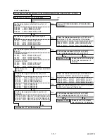
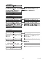
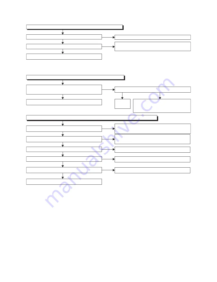
FLOW CHART NO.13
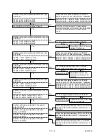
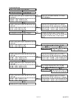
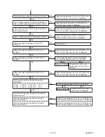
Hi-Fi audio can not be playbacked normally. (Hi-Fi E-E mode is normal.)
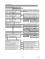
FLOW CHART NO.14
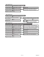
Hi-Fi audio can not be recorded normally in the linear audio mode. (E-E mode is normal.)
Is the audio signal inputted into Pin(13,15,17) of IC301?
Does the Bias oscillation circuit operate normally?
Is the audio signal outputted to Pin(11) of IC301?
Is the Playback Envelope signal outputted to
Pin(33) of IC451?
Replace IC301.
Is CN504 and the connected cable normal?
Is the Hi-Fi-H-SW signal inputted into to Pin(39) of IC451?
Yes
Yes
Yes
Is the audio signal outputted to Pin(100) of IC301?
Yes
Yes
Replace ACE head assembly.
Yes
Yes
No
No
No
No
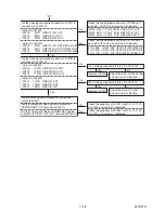
Check the Hi-Fi-H-SW line between
Pin(39) of IC451 and Pin(19) of
IC501, and service it if defective.
Check the line between Pin(78) of IC451 and
Pin(13,15,17) of IC301, and service it if defective.
Check the Bias oscillation circuit (Q401,Q403,
Q404,Q405,Q406) and service it if defective.
Replace
IC451.
Replace IC451.
No
Replace IC301.
No
Replace CN504 and the connected cable.
No
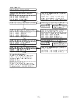
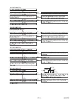
FLOW CHART NO.12
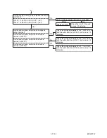
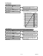
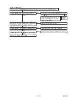
Hi-Fi audio can not be recorded normally. (E-E mode is normal.)
Is the REC FM signal outputted to Pin(26) of IC451?
Is the REC FM signal outputted to Pin(8) of CN251?
Replace the Cylinder Assembly.
Yes
Yes
No
Replace IC451.
No
Check the line between Pin(8) of CN251 and
Pin(26) of IC451, and service it if defective.
Summary of Contents for DRVR-B778S
Page 17: ...1 6 5 E9G01DC Fig D10 20 Deck Pedestal 21 Front Bracket R S 19 S 19 S 19 S 19 S 20...
Page 56: ...1 13 3 E9G10SCM1 Main 1 9 Schematic Diagram VCR Section...
Page 58: ...1 13 5 E9G10SCM3 Main 3 9 Schematic Diagram VCR Section...
Page 59: ...1 13 6 E9G10SCM4 Main 4 9 Schematic Diagram VCR Section...
Page 60: ...1 13 7 E9G10SCM5 Main 5 9 Schematic Diagram VCR Section...
Page 61: ...1 13 8 E9G10SCM6 Main 6 9 Front Jack Schematic Diagram VCR Section...
Page 62: ...1 13 9 E9G10SCM7 Main 7 9 Schematic Diagram VCR Section...
Page 63: ...1 13 10 E9G10SCM8 Main 8 9 Schematic Diagram VCR Section...
Page 64: ...1 13 11 E9G10SCM9 Main 9 9 Schematic Diagram VCR Section...
Page 66: ...1 13 13 E9G10SCRJ Rear Jack Schematic Diagram VCR Section...
Page 67: ...1 13 14 E9G10SCAFV AFV Schematic Diagram VCR Section...
Page 87: ...1 18 2 E9G01PEX Packing X4 S2 S2 S3 S2 A14 S1 S5 S5 S2 X9 X3 S9 X2 X1 X31 X43 X22 X20 S10...
Page 104: ...DRVR B778S E9G10BD 2007 07 23...

