background image

10-16

J124

C1500

GND

J125

C1501

GND

J126

C1502

P-ON-H1

J127

C1503

KEY-IN1

J

128

C1504

AMP-L

J129

C1505

R213

JS305

R215

JS306

R216

JS307

R217

JS308

AMP-R

J130

C1700

R218

JS309

R601

C1701

R219

C1702

R602

R603

C1703

DVD-Pb

J134

R604

C1704

R605

C1705

2

1

10

11

CN201

P-ON+3.3V

J

136

RCV-IN

J137

R607

JS310

ALL+3.3V

J138

R608

LED1

J139

R609

R222

R223

R226

PROTECT1

J140

R228

R610

DVD-Y

J141

R611

R229

GND

J142

R806

R612

J143

R807

GND

J

144

-7.5V

J145

R616

PROTECT2

J146

J147

J148

D1500

ALL+3.3V

J149

D1501

D1502

D1503

D1504

R235

R236

J150

R1504

P-ON+5.0V

J151

R1505

J152

R1506

J153

R1507

GND

J154

D1700

R1508

J155

C201

D1701

R1509

J156

D1702

LCD+12.5V

J157

D1703

LCD+12.5V

J158

C204

D1704

J159

C205

C207

R244

R1704

C208

R245

R1705

TU301

C209

R1706

TU302

R1707

R630

J160

R1

70

8

TU+5.0V

J161

C401

R631

R1709

PROTECT2

J162

GND

J163

J164

R634

J165

R635

GND

J166

PROTECT1

J167

R637

R250

GND

J168

CN1550

R638

P-ON-H1

J169

R252

R253

C217

R254

C218

FH601

C601

C602

FH602

C603

P-ON 3.3V

J170

C604

R834

C605

GND

J172

C606

VGH+25.6V

J173

C607

GND J174

C608

DIF -

J175

C1551

DIF +

J176

C1552

VGL-5.5V

J177

GND

J178

Q1550

C1554

J179

Q1551

C1555

R649

C803

C805

C806

R650

BL-ADJ.

J181

C1751

R651

GND

J182

C1752

R652

PROTECT3

J183

DRIVE+12.5V

J184

Q1750

C1754

R655

BL-SW

J185

Q1751

C1755

R656

GND

J186

J187

P-ON+3.3V

J188

R659

GND

J189

C812

C813

VGL-5.5V

J190

VCOM

J191

R661

LCD+12.5V

J192

R662

P-ON+5.0V

J193

R663

VCOM-PWM

J194

T1500

R664

GND

J195

R665

+7.0Vfor1.0V

J196

GND

GND

J198

D1550

P-ON+3.3V

J

199

D1551

D1552

D1553

D1554

C825

D1555

C631

C632

D1556

C827

D1557

C633

T1700

D1558

R670

D1559

R671

R1556

R672

C636

R1557

C638

D1750

D1751

C639

R675

D1752

R676

D1753

C830

D1754

D1560

C831

D1755

D1561

R679

D1756

D1562

C833

D1757

D1563

C834

D1758

C640

D1564

C641

D1759

D1565

R1756

D1567

R1757

C643

C838

R680

C645

R682

R683

C647

R684

D1760

C648

D1761

D201

C649

D202

D1762

D203

D1763

R688

D204

D1764

R689

D205

D1765

D206

D1767

D207

C650

D208

C652

C653

R690

C654

D401

D402

C656

D403

D210

D404

D211

D405

D212

D406

D407

D408

D409

CN872

C660

D601

L301

D602

D603

D604

D410

D605

D411

D606

D412

D413

D607

D414

D608

D415

D609

D416

D417

D418

BC301

D803

D804

D610

D805

Q901

D806

Q902

D807

Q903

Q904

D808

Q905

IC601

L901

T601

L902

J001

J002

INV.+31V

J003

INV.+31V

J004

1

9

IC801

J005

J006

J007

J008

C691

D631

J009

C692

D632

D633

GND

J200

D635

P-ON+5.0V

J201

GND

J202

D636

GND

J203

D637

C1003

7.0Vfor1.0V

J204

D638

J205

D639

J011

+3.5Vfor1.8V

J206

Q1002

C1006

-7.5V

J012

ALL+3.3V

J207

GND

J013

GND

J208

Q1004

+7.0V

J014

J015

RCV-IN

J209

Q1005

INV.+31V

J016

Q1006

GND

J017

Q1007

INV.+31V

J018

D640

Q1008

GND

J019

D641

Q1009

D642

D643

LED1

J210

D644

BC1001

D645

GND

J212

BC1002

D646

C1012

J213

C1013

BC1003

D647

+7.0V

J020

GND

J214

D648

Q1010

C1014

BC1004

J021

GND

J

215

D649

Q1011

5Vfor3.3V

J022

P-ON+3.3V

J216

Q1012

J217

5Vfor3.3V

J023

J219

J025

GND

J026

C1402

GND

J027

C1403

J028

D650

C1404

Q171

IC631

GND

J029

D651

Q1401

Q172

D652

D653

D

6

54

D655

D657

GND

J030

C1600

D659

J031

C1601

GND

J032

C1602

GND

J033

D1003

DRIVE+12.5V

J034

D1004

C1604

GND

J035

C1605

R1002

J036

D1006

J037

D1007

J038

D660

R1004

INV.+31V

J039

R1005

D1009

D662

D665

D666

INV.+31V

J040

D668

D1010

INV.+31V

J041

2

1

29

28

CN301

D1011

INV.+31V

J042

2

1

29

28

CN302

D1012

GND

J043

1

2

29

28

CN303

D1013

GND

J044

J045

J046

R1012

GND

J047

D670

DRIVE+12.5V

J048

J049

D1401

D1402

D1403

R904

R1018

D1404

R1019

D1406

R906

J050

GND

J051

J052

J053

J054

D1600

GND

J055

D1601

J056

R1022

D1602

J057

D1603

GND

J058

D1604

J059

1

2

28

29

CN702

R912

R1026

R913

R1027

R914

R1604

R1028

R1605

R1029

R1606

R1607

R917

GND

J060

R1608

GND

J061

R919

R1609

GND

J062

GND

J063

C303

GND

J064

R1030

J065

1

2

26

1

0

9

N

C

5

2

R1031

AMP-R-HP

J066

1

13

2

12

CN902

C306

J067

SP-GND

J068

GND

J069

R922

R923

R924

R925

R926

R927

J070

R928

J071

R929

AMP-L-HP

J072

JS632

J073

JS633

GND

J074

CN1650

D1045

SP+14V

J075

SP-GND

J076

R1042

INV.+31V

J077

SP-GND

J078

R930

J079

R932

R933

R1048

R1049

GND

J080

P-ON+9V

J081

C1651

GND

J082

C1652

GND

J083

GND

J084

Q1650

R1050

P-ON+9V

J085

Q1651

GND

J086

J087

P-ON-H1-SW

C1657

R1053

GND

J088

C1658

GND

J089

R172

R945

GND

J090

GND

J091

J092

J093

ALL+3.3V

J094

C910

DVD-AL

J095

GND

J098

GND

J099

C916

C917

C918

C919

T1600

S

A

6

0

1

D1650

D1651

R1071

C921

D1652

R1072

D1653

D1654

D1655

D1656

D1657

C928

D1658

D1659

R1656

R1657

D1660

D1661

D1662

D1663

D1664

Q201

D1665

Q202

D1667

Q203

Q205

Q206

Q207

Q208

Q209

D301

D302

D303

D304

Q401

Q402

Q211

Q215

Q601

Q602

JS1001

JS1002

JS1004

JS1005

Q801

L601

D901

D902

D903

D904

D905

D906

D907

D908

BC601

L804

M+10V

J100

P-ON+5V

J101

Q631

J102

Q632

Q633

P-ON+5V

J103

P-ON+5.0V

J104

Q634

J105

IC901

Q635

P-ON-H2

J106

Q636

Q637

DVD-MAIN-PWR

J108

GND

J110

LCD+12.5V

J111

Q641

J112

Q643

J113

J114

S-SW

J115

A-MUTE

J118

R201

JS101

R207

R208

J120

GND

J121

ALL+3.3V

J122

ALL+3.3V

J123

4

3

2

A

B

C

D

E

CAUTION

H.V

1

5

HOT

HOT

COLD

COLD

H.V

C

AUTION

H.V

CAUTION

COLD

AC601

HOT

TUNER

A

S

Q1001

D1005

J180

J096

D671

R241

Q210

R699

R698

R606

D656

C1603

D814

J197

CN1750

D813

J097

JS103

J171

JS1003

J109

J107

J116

1

8

CN102

JS102

C1653

C1553

C

1

5

5

0

C1650

C1753

C1750

F601

4A/125V

SCL

SDA

IF-AGC

SP-GND

LED-R

GND

DVD-LED

ALL+3.3V

RIPPLE REJECTION

AMP-R-HP

AMP-L-HP

P-ON-H2

+7.0V

+7.0V

INV.+31V

+7.0V

INV.+31V

INV.+31V

Operation

+31V

+31V

INV3 FB

INV2 FB

FET2 S

FB V

FB V

INV1 FB

for RT

+IN3

FET2 D

FET1 D

FET1 S

FET1 S

FET1 G

FET2 G

C1

C2

REF

REF

D+12.5V3

LCD+12.5V

LCD SW

P-ON+3.3V SW

CN801A

FET3 S

FET6 D

FET5 D

FET4 D

FET3 D

for RESET

for All+3.3V

GND

GND

+7.0V

P-ON+9.0V

INV+32 2

from Protect1

DVD-LED

+12.5V

LCD SW

LCD SW

for RESET

from P-ON-H2

from P-ON-H2

from P-ON-H2

from P-ON-H2

GND

PANEL+24.5V

TU+5V

32V-A

32V-S

5V-A

5V-S

GND

Q640

for A

for S

TU+5V

D611

P15V

3.5V

GND

S14V

5.0V

7.0V

31V

-7.5V

R401

R402

R403

Q1500

R404

R405

R211

JS301

C1506

R406

R212

C1507

R407

JS303

R408

R214

JS304

R409

Q1700

R411

C1706

R412

C1707

R413

R414

R220

R1105

R221

R1106

R1107

R224

R1109

R225

R802

R227

R803

R1110

R808

R230

R231

R232

R233

R810

R1500

R234

R811

R1501

R1502

R813

R1503

R237

R814

R238

R239

R817

R819

C202

R1700

R240

R1701

R1702

C206

R242

R1703

R820

R821

R822

R823

R824

R825

R826

C402

R632

R633

C210

C211

C212

R636

C213

C214

R251

C215

R639

C216

R830

R831

C219

R832

R833

R640

R641

R836

R642

R837

R643

R838

C220

R644

C221

R645

R646

C222

R647

C223

R648

C224

C801

C225

C1556

C226

C1557

C227

C1558

R841

R842

C809

R653

R654

C1756

C1757

R658

C810

C1758

C816

C817

R660

C818

C819

R666

R667

R668

C821

R669

R1550

R1551

C826

R1552

R1553

C828

R1554

C829

R1555

R673

R674

R1558

R1559

R677

R1750

R678

R1751

C832

R1752

R1753

R1754

R1560

R1755

C644

R1758

R681

R1759

R685

R686

R1760

C651

L302

L303

C681

C682

C683

C684

IC803

C1004

C1005

Q1003

C1007

C1008

C1009

C1010

C1011

C1015

C1016

Q1013

C1017

Q1014

C1018

C1019

C1401

R302

R303

R304

R305

R306

Q1402

R307

C1020

C1021

C1022

C1023

Q1023

Q1024

Q1600

C1606

C1607

R313

R1003

R1006

R1007

R1008

R1009

IC1001

IC1002

R1014

R901

R1015

R902

R1016

R903

R1017

JS801

R905

R1401

JS802

R1402

JS803

R907

R1403

JS804

R908

R1404

JS805

R909

R1405

R1406

R1407

R1020

R1021

R1023

J634

R910

R1600

R1024

J635

R911

R1601

R1025

R1602

R1603

R915

R916

R918

C302

C305

R1032

R1033

R920

R1034

C309

R921

R1035

R1036

R1037

C310

C311

C314

C315

R1043

R1044

R931

R1045

R1046

R1047

R934

R935

R936

R937

R938

R939

C901

R1051

R1052

C902

C903

R940

C904

R1054

R171

R941

C905

C1659

R1055

R942

C906

R1056

R943

R173

C907

R174

C908

R1058

R175

C909

R1059

C1660

C1661

R1060

C911

R1061

C912

R1062

C913

R1063

C914

R1064

C915

R1065

R1066

R1067

R1068

R1069

C920

R1070

C922

C923

R1074

C924

R1650

R1075

C925

R1651

R1076

C926

R1652

C927

R1653

R1654

C929

R1655

R1658

R1659

C930

C931

R1660

IC902

Q638

Q639

R202

R203

R204

R205

R809

R815

R816

R818

R839

R840

C811

D809

D810

IC201

1

4

5

8

J117

J131

1

4

5

8

1

4

5

8

1

7

8

14

1

8

9

16

WF1

PIN 4 OF 
CN302

WF3

PIN 6 OF 
CN302

WF1

PIN 4 OF 
CN302

WF3

PIN 6 OF 
CN302

WF2

PIN 8 OF 
CN302

WF7

PIN 13 OF 
CN302

WF4

PIN 15 OF 
CN302

WF5

PIN 17 OF 
CN302

WF6

PIN 19 OF 
CN302

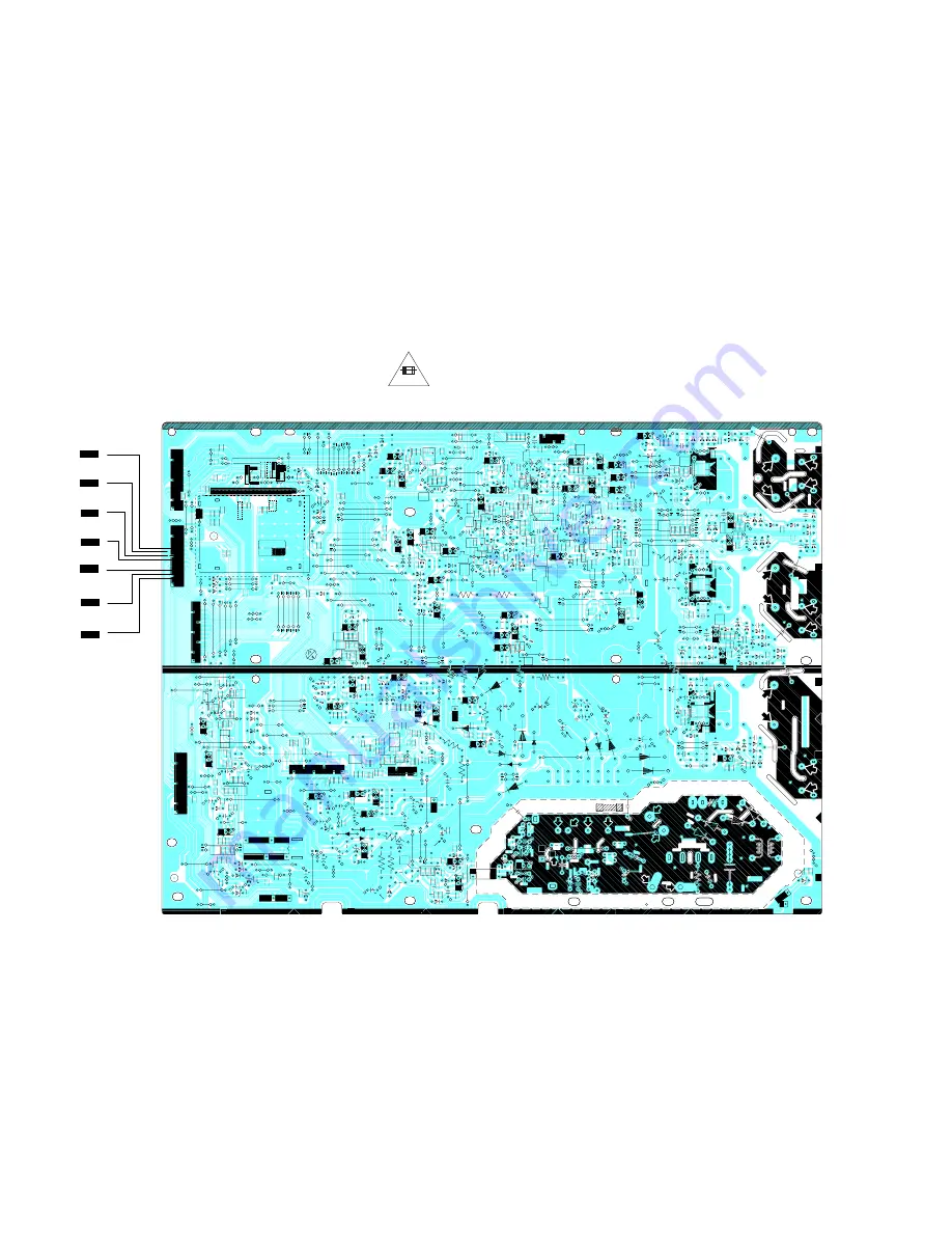
Main CBA Bottom  View

BA0171F01013

NOTE:

The voltage for parts in hot circuit is measured using 
hot GND as a common terminal.

Because a hot chassis ground is present in the power supply 
circuit, an isolation transformer must be used when repairing.
Also, in order to have the ability to increase the input slowly, 
when troubleshooting this type of power supply circuit, 
a variable isolation transformer is required. 

CAUTION !

Fixed voltage (or Auto voltage selectable) power supply circuit is used in this unit. 
If Main Fuse (F601) is blown , check to see that all components in the power supply 
circuit are not defective before you connect the AC plug to the AC power supply. 
Otherwise it may cause some components in the power supply circuit to fail.  

For continued protection against risk of fire, 
replace only with same type  4 A, 125V fuse.

CAUTION ! :

ATTENTION : 

Utiliser un fusible de rechange de même type de  4A, 125V.

4A/125V

Summary of Contents for FL10.1

Page 1: ...ange without notice Funai reserves the right to change the content herein without the obligation to notify any person or organization of such changes with the design is a registered trademark of Funai...

Page 2: ...quipment It also is important to understand that these CAUTIONS and NOTICES ARE NOT EXHAUSTIVE Funai could not possibly know evaluate and advice the service trade of all conceivable ways in which serv...

Page 3: ...net Disassembly Instructions 4 1 Electrical Adjustment Instructions 5 1 How to Initialize the LCD TV 6 1 Firmware Renewal Mode 7 1 Troubleshooting 8 1 Block Diagrams 9 1 Schematic Diagrams CBA and Tes...

Page 4: ...m dBm 76 0 76 0 76 4 Description Condition Unit Nominal Limit 1 Native Pixel Resolution Horizontal Vertical pixels pixels 1366 768 2 Brightness w filter cd m2 280 3 Viewing Angle Horizontal Vertical 8...

Page 5: ...m any AC source connect an electrical jumper across the two AC plug prongs Place the instrument AC switch in the on position Connect one lead of an ohmmeter to the AC plug prongs tied together and tou...

Page 6: ...is not isolated from the AC power line The two ground systems are electrically separated by insulation material that must not be defeated or altered 5 Observe original lead dress Take extra care to a...

Page 7: ...PVC tubing 3 Spacers 4 Insulators for transistors E When replacing AC primary side components transformers power cord etc wrap ends of wires securely about the terminals before soldering F Observe tha...

Page 8: ...exposed accessible parts RF terminals antenna terminals video and audio input and output terminals microphone jacks earphone jacks etc is lower than or equal to the specified value in the table below...

Page 9: ...he Flat Pack IC about 5 to 6 seconds Fig S 1 1 2 Remove the flat pack IC with tweezers while applying the hot air 3 Bottom of the flat pack IC is fixed with glue to the CBA when removing entire flat p...

Page 10: ...one using a sharp pin or wire to which solder will not adhere iron wire When heating the pins use a fine tip soldering iron or a hot air desoldering machine Fig S 1 4 3 Bottom of the flat pack IC is...

Page 11: ...g S 1 6 Note When using a soldering iron care must be taken to ensure that the flat pack IC is not being held by glue When the flat pack IC is removed from the CBA handle it gently because it may be d...

Page 12: ...d to remove any static electricity that may be charged on the body 2 Ground for Workbench Be sure to place a conductive sheet or copper plate with proper grounding 1 M on the workbench or other surfac...

Page 13: ...ollowing Reference Notes in the Table Step Loc No Part Removal Fig No Remove Unhook Unlock Release Unplug Unclamp Desolder Note 1 Stand Assembly D1 3 S 1 2 Rear Cabinet D1 9 S 2 2 S 3 S 4 3 S 5 3 Jack...

Page 14: ...4 2 FL10 1DC 2 Rear Cabinet S 1 1 Stand Assembly S 2 S 2 S 5 S 2 S 4 S 3 S 2 S 2 S 2 Fig D1...

Page 15: ...t 8 Stand Holder 7 Main CBA 9 LCD Module Assembly 14 Junction A CBA 12 Junction C CBA 13 Junction B CBA 15 Function CBA 16 Front Cabinet 10 Speaker Holder 11 Speaker 3 Jack Holder D 5 Jack Holder A S...

Page 16: ...750 CN3902 CN3702 CN3701 Digital Main CBA Unit CN102 CN101 CN101A CN702 AC CORD CN302 CN701 CN861A CN861B CL861 CN301 CN101B Junction C CBA Junction A CBA Junction B CBA Function CBA To LCD Module Ass...

Page 17: ...quipment is available Test Equipment Required 1 NTSC Pattern Generator Color Bar W White Window Red Color Dot Pattern Gray Scale Monoscope Multi Burst 2 Remote control unit 3 Color Analyzer How to set...

Page 18: ...The optical receptor must be set perpendicularly to the LCD Panel surface 3 Enter the Service mode 4 Press 3 button on the remote control unit 5 Press CH X Y buttons on the remote control unit so that...

Page 19: ...5 CUTOFF Press 1 button to select COR for Red Cutoff adjustment Press 3 button to select COB for Blue Cutoff adjustment DRIVE Press 4 button to select DR for Red Drive adjustment Press 6 button to se...

Page 20: ...To put the program back at the factory default initialize the LCD TV using the following procedure 1 Turn the power on 2 Enter the service mode To cancel the service mode press button on the remote c...

Page 21: ...the power off and turn the power on again Note When the Factory Upgrade is used after restarting TV shift to initial screen menu in service mode INITIALIZED will appear on the upper right of the scre...

Page 22: ...secondary side and service it if defective After servicing replace the fuse When the output voltage fluctuates FLOW CHART NO 3 Does the photocoupler circuit on the secondary side operate normally No Y...

Page 23: ...r of Q201 Yes Check C631 D631 D668 and their periphery circuit and service it if defective P ON 7V is not output FLOW CHART NO 8 Is approximately 7V voltage supplied to the cathode of D641 Check C641...

Page 24: ...service it if defective Check Q638 Q639 P ON H2 line and their periphery circuit and service it if defective No FLOW CHART NO 13 Replace Q640 P ON 3V is not output FLOW CHART NO 11 Is approximately 3V...

Page 25: ...mately 34V voltage supplied to the collector of Q634 Yes Replace IC631 Check C636 D636 D637 and their periphery circuit and service it if defective Check Q202 Q203 D204 P ON H1 line and their peripher...

Page 26: ...e control unit Yes Replace Digital Main CBA Unit When pressing each switches SW104 SW109 do the voltage of Pin 29 of CN302 increase Yes The key operation is not functioning FLOW CHART NO 1 Are the con...

Page 27: ...nput FLOW CHART NO 4 Are the DIF signal inputted to Pin 26 28 of CN302 Yes Replace Digital Main CBA Unit or LCD Module Assembly Replace Digital Main CBA Unit or LCD Module Assembly Pin 6 S VIDEO C Pin...

Page 28: ...803 and service it if defective Are the audio L R signals outputted to Pin 1 7 of IC803 No Yes Replace IC803 No Check SP861 SP862 and their periphery circuit and service it if defective Are the audio...

Page 29: ...ctive Are the audio L R signals outputted to Pin 1 7 of IC803 No Yes Replace IC803 No Check SP861 SP862 and their periphery circuit and service it if defective Are the audio L R signals inputted to Pi...

Page 30: ...if defective No No Are the audio L R signals outputted to Pin 4 6 of IC801 Check IC801 and their periphery circuit and service it if defective No Yes Are the audio L R signals inputted to Pin 6 8 of C...

Page 31: ...Q171 K3 IC3301 MAIN MICRO CONTROLLER DIGITAL MAIN CBA UNIT CN3702 CN3702 CLKOUT 25M CLKIN 25M X3101 25MHz OSC U1 V1 CLKOUT 32K CLKIN 32K X3102 32 768kHz OSC N2 N1 PROTECT3 M2 VCOM PWM M4 PROTECT2 L3...

Page 32: ...C Y JK752 VIDEO IN S VIDEO SW IN 19 19 COM VIDEO Y IN 20 20 COM VIDEO Pb IN 18 18 COM VIDEO Pr IN 16 16 MAIN CBA TU302 DIF OUT1 11 DIF OUT2 10 TUNER UNIT IF AGC 9 CN302 CN3702 DIF OUT1 26 26 IF AGC 2...

Page 33: ...CONTROL DRIVE CN302 CN3702 AUDIO MUTE 20 20 JK841 DIGITAL AUDIO OUT COAXIAL Q841 Q771 Q722 BUFFER SPDIF 2 2 SPDIF 23 23 Q801 CONTROL LOGIC 3 10 9 13 IC803 OP AMP 1 3 7 5 DRIVE AUDIO L AUDIO R TO DIGIT...

Page 34: ...7 26 27 23 24 20 21 17 18 8 7 11 10 14 13 5 4 1 2 9 4 6 1 3 10 12 16 15 7 9 4 6 1 3 10 12 16 15 JK3702 TMDS D0 TMDS D0 TMDS D1 TMDS D1 TMDS D2 TMDS D2 TMDS CLOCK TMDS CLOCK SDA SCL TMDS CLOCK TMDS CLO...

Page 35: ...TROL SWITCH CURRENT CONTROL SWITCH Q1700 CURRENT CONTROL SWITCH OVER VOLTAGE PROTECTOR OVER VOLTAGE PROTECTOR OVER VOLTAGE PROTECTOR OVER VOLTAGE PROTECTOR Q1550 OVER VOLTAGE PROTECTOR Q1551 OVER VOLT...

Page 36: ...V P ON 7V AL 3 3V P ON 3 3V P ON 5V LCD MODULE ASSEMBLY DIGITAL MAIN CBA UNIT PANEL 7 1V 8 P ON 3 3V 19 20 P ON 3 3V 6 7 PANEL 24 5V 4 PANEL 13V 2 3 AL 3 3V 21 22 16 10 P ON 7V 16 P ON 3V 10 P ON 5V 1...

Page 37: ...k fire or other hazards Notes 1 Do not use the part number shown on these drawings for ordering The correct part number is shown in the parts list and may be slightly different or amended since these...

Page 38: ...mended since the drawings were prepared 2 To maintain original function and reliability of repaired units use only original replacement parts which are listed with their part numbers in the parts list...

Page 39: ...10 3 FL10 1SCM1 Main 1 Schematic Diagram...

Page 40: ...10 4 FL10 1SCM2 Main 2 Schematic Diagram...

Page 41: ...10 5 FL10 1SCM3 Main 3 Junction B Schematic Diagram...

Page 42: ...fuse CAUTION ATTENTION Utiliser un fusible de rechange de m me type de 4A 125V 4A 125V CAUTION Fixed voltage or Auto voltage selectable power supply circuit is used in this unit If Main Fuse F601 is b...

Page 43: ...10 7 FL10 1SCJ Jack Junction C Schematic Diagram...

Page 44: ...10 8 FL10 1SCF Function Junction A Schematic Diagram...

Page 45: ...Main 1 Schematic Diagram The order of pins shown in this diagram is different from that of actual IC3301 IC3301 is divided into five and shown as IC3301 1 6 IC3301 6 6 in this Digital Main Schematic...

Page 46: ...l Main 2 Schematic Diagram The order of pins shown in this diagram is different from that of actual IC3301 IC3301 is divided into five and shown as IC3301 1 6 IC3301 6 6 in this Digital Main Schematic...

Page 47: ...l Main 3 Schematic Diagram The order of pins shown in this diagram is different from that of actual IC3301 IC3301 is divided into five and shown as IC3301 1 6 IC3301 6 6 in this Digital Main Schematic...

Page 48: ...l Main 4 Schematic Diagram The order of pins shown in this diagram is different from that of actual IC3301 IC3301 is divided into five and shown as IC3301 1 6 IC3301 6 6 in this Digital Main Schematic...

Page 49: ...l Main 5 Schematic Diagram The order of pins shown in this diagram is different from that of actual IC3301 IC3301 is divided into five and shown as IC3301 1 6 IC3301 6 6 in this Digital Main Schematic...

Page 50: ...hematic Diagram FL10 1SCD6 The order of pins shown in this diagram is different from that of actual IC3301 IC3301 is divided into five and shown as IC3301 1 6 IC3301 6 6 in this Digital Main Schematic...

Page 51: ...D666 INV 31V J040 D668 D1010 INV 31V J041 2 1 29 28 CN301 D1011 INV 31V J042 2 1 29 28 CN302 D1012 GND J043 1 2 29 28 CN303 D1013 GND J044 J045 J046 R1012 GND J047 D670 DRIVE 12 5V J048 J049 D1401 D14...

Page 52: ...D1664 Q201 D1665 Q202 D1667 Q203 Q205 Q206 Q207 Q208 Q209 D301 D302 D303 D304 Q401 Q402 Q211 Q215 Q601 Q602 JS1001 JS1002 JS1004 JS1005 Q801 L601 D901 D902 D903 D904 D905 D906 D907 D908 BC601 L804 M...

Page 53: ...8 5 2 J 8 0 1 J 8 0 2 J 8 0 4 J 8 0 5 J 8 0 6 J 8 0 7 J 8 0 8 J 8 1 0 J 8 1 2 J 8 1 3 J 8 1 4 J K 7 1 1 J 8 1 5 J 8 1 6 J 8 1 7 J 8 1 8 J 8 1 9 Q 7 7 1 Q 7 2 2 Q 7 7 3 J 8 2 0 Q 7 7 4 J 8 2 1 C N 7 0...

Page 54: ...8 4 1 J K 7 2 2 J K 7 2 1 J 8 1 1 J 8 2 2 G N D D 7 0 9 D 7 0 6 D 7 0 5 P O N 9 V P O N 9 V A M P R S P C N 8 6 1 B C L 8 6 1 C N 8 6 2 B C L 8 6 2 P b P b P b C 1 1 1 C 1 0 4 R 1 1 0 R 1 0 7 C 1 0 6...

Page 55: ...veform check points Shown in Schematic Diagram CVBS 0 2V 20 s WF1 Pin 4 of CN302 S VIDEO Y 0 2V WF2 Pin 8 of CN302 20 s S VIDEO C 0 2V WF3 Pin 6 of CN302 20 s AUDIO 0 1V 0 5ms WF7 Pin 13 of CN302 VIDE...

Page 56: ...3701 CN301 23 19 21 15 17 22 20 18 16 14 10 12 6 8 13 11 9 7 5 1 3 4 1 5 3 9 7 2 4 6 8 10 14 12 18 16 11 13 15 17 19 23 21 20 2 P ON H2 AUDIO L OUT NU GND AUDIO R OUT NU PROTECT3 AMP L OUT GND AMP R O...

Page 57: ...01 Function CBA SP861 SP862 Main CBA B8 A3 Stand Assembly Jack CBA L2 L2 B3 B3 L1 L1 L17 B13 L13 B14 B2 S5 L3 B44 B7 B7 L12 L12 L12 L3 L3 L11 A4 LCD1 L9 L9 L3 L4 L4 L3 L3 A10 L1 L1 L8 B8 L1 L3 L3 L3 J...

Page 58: ...13 2 FL10 1PEX Packing S3 S1 Tape Packing Tape Packing Tape Packing Tape Packing Tape S2 S3 X1 Some Ref Numbers are not in sequence L17 X2 S4 X8 X6 S6 S5 Stand Assembly X4 X3 FRONT FRONT Tape...

Page 59: ...01 WIRE ASSEMBLY 29PIN FFC 29PIN 50MM WX1A94F0 101 CL3701 WIRE ASSEMBLY 29PIN FFC 29PIN 50MM WX1A94F0 101 CL3702 WIRE ASSEMBLY 29PIN FFC 29PIN 70MM WX1A94F0 111 CL3902 WIRE ASSEMBLY 24PIN FFC 24PIN 80...

Page 60: ...M CE1EMZNDL102 C645 POLYESTER FILM CAP PB FREE 0 0022 F 100V J CA2A222DT018 C647 ELECTROLYTIC CAP 100 F 10V M H7 CE1AMAVSL101 C649 ELECTROLYTIC CAP 220 F 10V M H7 CE1AMAVSL221 C650 ELECTROLYTIC CAP 22...

Page 61: ...DE ZENER 5V6BSB T26 NDTB5R6BST26 D210 SWITCHING DIODE 1SS133 T 77 QDTZ001SS133 D211 SWITCHING DIODE 1SS133 T 77 QDTZ001SS133 D212 SWITCHING DIODE 1SS133 T 77 QDTZ001SS133 D303 DIODE ZENER 5V6BSB T26 N...

Page 62: ...T 77 QDTZ001SS133 D1762 SWITCHING DIODE 1SS133 T 77 QDTZ001SS133 D1763 SWITCHING DIODE 1SS133 T 77 QDTZ001SS133 D1764 SWITCHING DIODE 1SS133 T 77 QDTZ001SS133 D1765 SWITCHING DIODE 1SS133 T 77 QDTZ00...

Page 63: ...2 2k RRXAJR5Z0222 Ref No Description Part No R411 CHIP RES 1 10W J 22k RRXAJR5Z0223 R412 CHIP RES 1 10W J 22k RRXAJR5Z0223 R413 CHIP RES 1 10W J 22k RRXAJR5Z0223 R601 GLASS GLAZE RES 1 2W J 1M RXX2JZ...

Page 64: ...R1037 CHIP RES 1608 1 10W 0 RRXAZR5Z0000 R1043 CHIP RES 1 10W J 12k RRXAJR5Z0123 Ref No Description Part No R1044 CHIP RES 1 10W F 2 7k RRXAFR5H2701 R1045 CHIP RES 1 10W F 1 2k RRXAFR5H1201 R1048 RES...

Page 65: ...ER HVT 179 LTZ3PZ0XB012 T1600 TRANS INVERTER HVT 179 LTZ3PZ0XB012 T1700 TRANS INVERTER HVT 179 LTZ3PZ0XB012 TU302 TUNER UNIT ATSC TDAU4 D05A UTNATS0AL002 Ref No Description Part No Ref No Description...

Page 66: ...CHIP RES 1 10W J 2 2k RRXAJR5Z0222 R797 CHIP RES 1 10W J 2 2k RRXAJR5Z0222 R843 CHIP RES 1 10W J 110 RRXAJR5Z0111 R844 CHIP RES 1 10W J 220 RRXAJR5Z0221 R845 CHIP RES 1 10W J 100k RRXAJR5Z0104 Ref No...

Page 67: ...BLY 8PIN 8PIN 150MM WX1A9170 001 Ref No Description Part No JUNCTION B CBA MJC D Consists of the following CONNECTOR CN862B 242SERIESCONNECTORTUC P04X B1WHT ST JCTUB04TG002 MISCELLANEOUS CL862 WIRE AS...

Page 68: ...servicing NOTE Parts that are not assigned part numbers are not available Different parts from the original model LC220SS1 Ref No Description Part No A1 FRONT CABINET A0175UH 1EM025433 A3 CONTROL PLAT...

Page 69: ...replacing any of these components read carefully the product safety notice in this service manual Don t degrade the safety of the product through improper servicing NOTE Parts that are not assigned pa...

Page 70: ...s that are not assigned part numbers are not available Different parts from the original model LC220SS1 Ref No Description Part No A1 FRONT CABINET A0173UH 1EM124953 A3 CONTROL PLATE A91N3UH 1EM325763...

Page 71: ...replacing any of these components read carefully the product safety notice in this service manual Don t degrade the safety of the product through improper servicing NOTE Parts that are not assigned pa...

Page 72: ...15 1 FL10 1REV REVISION HISTORY Chassis FL10 1 2010 03 30 LC220SS1 added 2010 04 23 LC220EM1 added 2010 05 06 LC220SL1 added TBD 22MF330B F7 added...

Reviews: