1-13-8
E3TFGTR
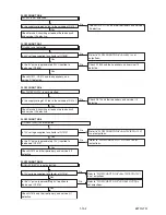
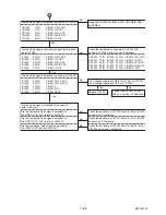
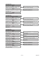
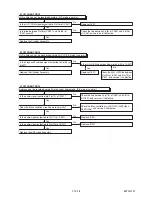
Are the video signals outputted to each pin of IC1509?
Yes
Yes
No
Check the periphery of JK1504 from Pin (30) of IC1509
and service it if defective.
Check the periphery of JK2001 from Pin (22) of IC1509
and service it if defective.
Check the periphery of JK1505 from Pin (38, 39, 40) of
IC1509 and service it if defective.
Are the video signals outputted to the specific
output terminal?
No
No
No
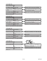
Are the composite video signals outputted to
the VIDEO OUT (AV1) terminal (JK1504)?
Are the composite video signals outputted to
the VIDEO OUT (AV2) terminal (JK2001)?
Are the component video signals outputted to
the VIDEO OUT terminal (JK1505)?
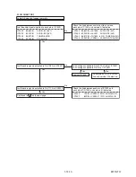
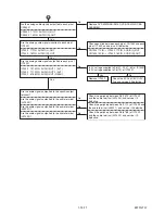
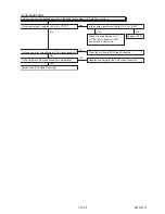
Are the video signals outputted to each pin of CN1502?
Replace DVD MECHANISM & DVD/HDD MAIN CBA
ASSEMBLY.
Check the line between each pin of CN1502 and
each pin of IC1509, and service it if defective.
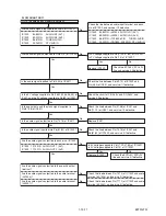
Are the video signals shown above inputted into each
pin of IC1509?
Yes
No
No
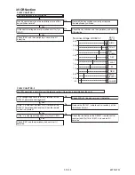
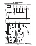
CN1502
VIDEO-Y(I/P)-OUT
7PIN
CN1502
VIDEO-Y(I)-OUT
1PIN
CN1502
VIDEO-Pr/Cr-OUT
5PIN
CN1502
VIDEO-Pb/Cb-OUT
3PIN
CN1502
VIDEO-C-OUT
VIDEO-Y(I/P)-OUT
VIDEO-Pr/Cr-OUT
VIDEO-Pb/Cb-OUT
VIDEO-C-OUT
9PIN
IC1509
VIDEO-Y(I/P)-OUT
51PIN
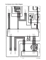
IC1509
VIDEO-Y(I)-OUT
55PIN
IC1509
VIDEO-Pr/Cr-OUT
52PIN
IC1509
VIDEO-Pb/Cb-OUT
53PIN
IC1509
VIDEO-C-OUT
57PIN
IC1509
VIDEO-OUT 1 (AV1)
30PIN
IC1509
VIDEO-OUT 2 (AV2)
22PIN
IC1509
VIDEO-Y
40PIN
IC1509
VIDEO-Pr/Cr
39PIN
IC1509
VIDEO-Pb/Cb
38PIN
CN1502
IC1509
7PIN
CN1502
IC1509
5PIN
CN1502
IC1509
3PIN
IC1509
9PIN
51PIN
VIDEO-Y(I)-OUT
CN1502
IC1509
1PIN
55PIN
52PIN
53PIN
57PIN
CN1502
A
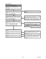
Check the ECO+5V, ECO+9V
line and service it if defective.
Replace IC1509.
Yes
No
Is 5V voltage supplied to Pin(27,29,47,63) of IC1509?
Is 9V voltage supplied to Pin(75) of IC1509?
Summary of Contents for TD6D-M101
Page 61: ...1 15 3 E3TFGSCAV1 AV 1 10 Schematic Diagram VCR Section...
Page 63: ...1 15 5 E3TFGSCAV3 AV 3 10 Schematic Diagram VCR Section...
Page 64: ...1 15 6 E3TFGSCAV4 AV 4 10 Schematic Diagram VCR Section...
Page 65: ...1 15 7 E3TFGSCAV5 AV 5 10 Schematic Diagram VCR Section...
Page 66: ...1 15 8 E3TFGSCAV6 AV 6 10 Schematic Diagram VCR Section...
Page 67: ...1 15 9 E3TFGSCAV7 AV 7 10 Schematic Diagram VCR Section...
Page 68: ...1 15 10 E3TFGSCAV8 AV 8 10 Schematic Diagram VCR Section...
Page 69: ...1 15 11 E3TFGSCAV9 AV 9 10 Schematic Diagram VCR Section...
Page 70: ...1 15 12 E3TFGSCAV10 AV 10 10 Schematic Diagram VCR Section...
Page 73: ...1 15 15 Rear Jack Schematic Diagram VCR Section E3TFGSCRJ...
Page 79: ...1 15 21 E3TFGSCD6 DVD HDD Main 6 7 Schematic Diagram DVD HDD Section...
Page 81: ...1 15 23 E3TFGSCDTV DTV Module Schematic Diagram DVD HDD Section...
Page 82: ...1 15 24 E3TFGSCSATA SATA Schematic Diagram...
Page 107: ...TD6D M101 E3TFGEH 2013 04 22...

