background image

1-13-1

W4PWF

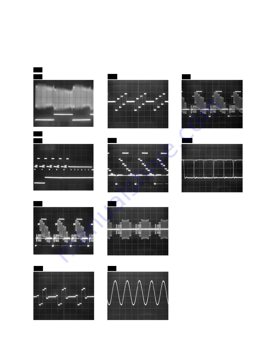
WAVEFORMS

WF8

AUDIO(L)-OUT

Pin 17 of CN1502

1V

0.5ms

WF5

VIDEO-Cb

Pin 3 of CN1502

0.2V

20

µ

s

WF4

VIDEO-Cr

Pin 5 of CN1502

0.2V

20

µ

s

SPDIF

1V

0.1

µ

s

WF10

Pin 3 of CN1501

WF6

Pin 7 of CN1502

VIDEO-Y

0.2V

20

µ

s

WF7

Pin 9 of CN1502

VIDEO-C

0.2V

20

µ

s

WF9

Pin 6 of IC1515

VIDEO-CVBS

0.5V

20

µ

s

WF2

WF3

UPPER

WF1

WF1

LOWER

J236

TP504

UPPER

LOWER

TP504

TP301

V-OUT 

0.5V

50

µ

s

RF-SW

5V

C-PB 
RF-SW

5V

5ms

0.2V

WF3

J236

V-OUT E-E

0.2V

20

µ

s

NOTE:

Input: COLOR BAR SIGNAL (WITH 1KHz AUDIO SIGNAL)

Summary of Contents for W4A-A4180DB

Page 1: ...D4180DB W4D D4180DB Main Section I Specifications I Preparation for Servicing I Adjustment Procedures I Schematic Diagrams I CBA s I Exploded views I Parts List When servicing the deck mechanism refe...

Page 2: ...Mode 1 9 1 Function Indicator Symbols 1 10 1 Block Diagrams 1 11 1 Schematic Diagrams CBA s and Test Points 1 12 1 Waveforms 1 13 1 Wiring Diagram VCR Section 1 14 1 Wiring Diagram DVD Section 1 14 2...

Page 3: ...de W O Burst 1 4 Video Color S N AM R P dB 37 41 SP Mode 1 5 Video Color S N PM R P dB 30 36 SP Mode 1 6 Resolution PB Line 230 245 SP Mode 2 Servo 2 1 Jitter Low sec 0 07 0 12 SP Mode 2 2 Wow Flutter...

Page 4: ...load Vp p 1 0 C Chrominance 75 load Vp p 0 3 2 AUDIO 2 1 Output Level Vrms 2 0 2 2 Frequency Response DVD VIDEO LPCM fs 96 kHz Hz 20 44 k fs 48 kHz Hz 20 20 k Audio CD fs 44 1 kHz Hz 20 20 k 2 3 Signa...

Page 5: ...y from the pickup lens when the diode is turned on Do not look directly at the laser beam CAUTION Use of controls and adjustments or doing procedures other than those specified herein may result in ha...

Page 6: ...cal for safety Replace only with part number specified B In addition to safety other parts and assemblies are specified for conformance with regulations applying to spurious radiation These must also...

Page 7: ...2 Leakage Current Test Confirm the specified or lower leakage current between B earth ground power cord plug prongs and externally exposed accessible parts RF termi nals antenna terminals video and a...

Page 8: ...achine then apply hot air to the Flat Pack IC about 5 to 6 seconds Fig S 1 1 2 Remove the flat pack IC with tweezers while applying the hot air 3 Bottom of the flat pack IC is fixed with glue to the C...

Page 9: ...by one using a sharp pin or wire to which solder will not adhere iron wire When heating the pins use a fine tip soldering iron or a hot air desoldering machine Fig S 1 4 3 Bottom of the flat pack IC i...

Page 10: ...s Fig S 1 6 Note When using a soldering iron care must be taken to ensure that the flat pack IC is not being held by glue When the flat pack IC is removed from the CBA handle it gently because it may...

Page 11: ...ed to remove any static electricity that may be charged on the body 2 Ground for Workbench Be sure to place a conductive sheet or copper plate with proper grounding 1 M on the workbench or other surfa...

Page 12: ...o the Deck Mechanism Assembly and press the PLAY VCR button The tape will be loaded into the Deck Mechanism Assembly Make sure the power is on connect TP501 S INH to GND This will stop the function of...

Page 13: ...4 5 Front Jack CBA D3 Jack Earth Plate 6 DVD Mechanism DVD Main CBA Assembly D4 4 S 5 CN101 CN701 4 7 Dust Cover D4 8 Rear Panel Unit D5 4 S 6A 2 S 6B 3 S 7 S 8 CN1503 9 Fan Holder D6 3 S 9 10 Motor...

Page 14: ...D9 Then install the Deck Assembly while aligning the hole of Cam Gear with the pin of LD SW the shaft of Cam Gear with the hole of LD SW as shown in Fig D9 4 The DVD Mechanism DVD Main CBA Assem bly i...

Page 15: ...7 S 7 S 7 CN1503 S 8 8 Rear Panel Unit Fig D6 S 9 11 Rear Panel 10 Motor DC Fan 9 Fan Holder CN1504 Fig D7 S 11 S 10 12 Power Supply CBA 13 PCB Holder Fig D8 S 12 S 15 S 16 S 14 S 14 S 13C PCB Washer...

Page 16: ...E Head BOTTOM VIEW Lead connections of Deck Assembly and Main CBA Desolder From Capstan Motor Assembly Printing side Desolder From Cylinder Assembly From ACE Head Assembly Lead with blue stripe Lead w...

Page 17: ...1 6 5 E9G02DC Fig D10 20 Deck Pedestal 21 Front Bracket R S 19 S 19 S 19 S 19 S 20...

Page 18: ...the Front Bracket 4 Remove the DVD Mechanism DVD Main CBA Assembly 5 Unhook two places and detach the Dust Cover 6 Rotate the gear in the direction of the arrow manually as shown below until the tray...

Page 19: ...0 001 50V Div F Range DC AC 20MHz 2 Alignment Tape FL6A Head Switching Position Adjustment Purpose To determine the Head Switching position during playback Symptom of Misadjustment May cause Head Swit...

Page 20: ...tializing is completed the DVD recorder exits the Version display mode and turns off the power automatically To move into the Normal mode from the Version display mode press RETURN button on the remot...

Page 21: ...scribed as follows 5 After updating is finished the tray opens automatically At this time no button is available 6 Pull out the AC code once then insert it again Fig a Version Up Mode Screen Firmware...

Page 22: ...E When reel or capstan mechanism is not functioning correctly A R is displayed on a TV screen Refer to Fig 1 When tape loading mechanism is not func tioning correctly A T is displayed on a TV screen R...

Page 23: ...able 14 Cannot write the data after recovering SMALL VMGI 15 Cannot write the data after DVD R Reverse Track 16 An error occurs in Finalize Close 17 An error occurs in Rec Stop Close 18 An error occur...

Page 24: ...cessary titles 34 There is not space to record field of control information 10 You cannot record on the disc as Power Calibration Area is full Insert a new disc 35 PCA is Full in REC start 4 This disc...

Page 25: ...BUS SCL D V SYNC D REC H RF SW H A SW C ROTA IIC BUS SDA H A COMP V ENV DVD AUDIO MUTE DVD SCART AUDIO MUTE 30 C SYNC C SYNC IIC BUS SCL LD SW 9 AL 5V SW507 LD SW AL 5V D555 S LED TP501 RM1501 SENS IN...

Page 26: ...RACKING FOCUS PICK UP SLED MOTOR M REC VIDEO SIGNAL PB VIDEO SIGNAL REC AUDIO SIGNAL PB AUDIO SIGNAL D A LPC CN1001 CN701 SPINDLE MOTOR M CN1002 CN301 3 3V IC701 VIDEO DECODER DECODER A D 45 50 U4 W1...

Page 27: ...2 VIDEO COM VIDEO R 2 4 5 6 IC301 VIDEO SIGNAL PROCESS HEAD AMP IC501 OSD VCR VIDEO VCR VIDEO DUB VCR DVD DUBBING DVD VIDEO DUB PB EE VIDEO REC VIDEO SIGNAL SERIAL DECORDER 48 50 50 52 96 95 94 93 90...

Page 28: ...CN1502 CN1505 2 2 FRONT Y IN 1 1 FRONT C IN 4 4 FRONT VIDEO IN CN1201 Q1520 Q1521 BUFFER VIDEO SW1 IC1518 VIDEO INPUT SELECT IC1508 SW 29 33 32 28 1 3 5 30 31 6dB AMP CONTROL LOGIC SW CTL 6dB AMP DRI...

Page 29: ...AMP 2dB AMP LPF DRIVER 6 8dB AMP 6dB DRIVER 4dB AMP 2dB AMP LPF DRIVER 3 1 7 13 4dB AMP 2dB AMP LPF DRIVER 11 4dB AMP 2dB AMP LPF DRIVER 6 10 4dB AMP 2dB AMP LPF DRIVER 8 1 15 15 1 2 4 9 10 11 3 5 IC...

Page 30: ...MUTE 11 6 PB ON SP LP ON P TUNER IN2 IN1 R ALC DET ALC IC301 AUDIO SIGNAL PROCESS HEAD AMP 15 13 17 4 AUDIO PB REC CN504 3 A COM 1 AE H 2 AE H FE H AUDIO HEAD AUDIO ERASE HEAD ACE HEAD ASSEMBLY FE HE...

Page 31: ...MP IC1513 SW IC1508 OP AMP OP AMP 2 6 1 7 TO SERVO SYSTEM CONTROL BLOCK DIAGRAM TO Hi Fi AUDIO BLOCK DIAGRAM WF8 Q1537 Q1507 MUTE ON Q1538 MUTE ON Q2002 MUTE ON Q2003 MUTE ON IF SIGNAL PROCESS CN1506...

Page 32: ...R DVD VCR DUBBING VCR AUDIO R DVD AUDIO L VCR AUDIO L LIM 80 N A PB Hi Fi H SW AUDIO MUTE 2 A MODE TO AUDIO BLOCK DIAGRAM TO AUDIO INPUT OUTPUT SELECT BLOCK DIAGRAM TO AUDIO INPUT OUTPUT SELECT BLOCK...

Page 33: ...25 25 AL 3V 26 26 AL 3V 31 31 AL 4V 32 32 AL 4V 34 34 F1 33 33 F2 2 2 AL 12V 3 3 AL 12V 6 6 FAN AL 12V 7 7 FAN AL 12V 8 8 FAN AL 12V TO SERVO SYSTEM CONTROL BLOCK DIAGRAM TO SERVO SYSTEM CONTROL BLOCK...

Page 34: ...stitute replacement parts that do not have the same safety characteristics as specified in the parts list may create shock fire or other hazards Notes 1 Do not use the part number shown on these drawi...

Page 35: ...acement parts which are listed with their part numbers in the parts list section of the service manual 4 Voltage indications for PLAY and REC modes on the schematics are as shown below 5 How to read c...

Page 36: ...1 12 3 E9G00SCM1 Main 1 9 Schematic Diagram VCR Section Comparison Chart of Models and Marks MODEL MARK W4A A4180DB A W4A D4180DB B W4D D4180DB C...

Page 37: ...g c d e f g h h i a b a b a b a b a b FL601 MATRIX CHART REPEAT PM REC VCD VCR DVD R XP SP LP EP SLP P SCAN SEP W CD T C 5G 4G 3G 2G 1G 7G 6G a d g h h g c b e f REPEAT PM REC VCD VCR DVD R XP SP LP...

Page 38: ...1 12 5 E9G00SCM3 Main 3 9 Schematic Diagram VCR Section Comparison Chart of Models and Marks MODEL MARK W4A A4180DB A W4A D4180DB B W4D D4180DB C...

Page 39: ...1 12 6 E9G00SCM4 Main 4 9 Schematic Diagram VCR Section...

Page 40: ...1 12 7 E9G00SCM5 Main 5 9 Schematic Diagram VCR Section...

Page 41: ...1 12 8 E9G00SCM6 Main 6 9 Front Jack Schematic Diagram VCR Section...

Page 42: ...1 12 9 E9G00SCM7 Main 7 9 Schematic Diagram VCR Section...

Page 43: ...1 12 10 E9G00SCM8 Main 8 9 Schematic Diagram VCR Section...

Page 44: ...1 12 11 E9G00SCM9 Main 9 9 Schematic Diagram VCR Section...

Page 45: ...k to see that all components in the power supply circuit are not defective before you connect the AC plug to the AC power supply Otherwise it may cause some components in the power supply circuit to f...

Page 46: ...1 12 13 E9G00SCRJ Rear Jack Schematic Diagram VCR Section...

Page 47: ...1 12 14 E9G00SCAFV AFV Schematic Diagram VCR Section Comparison Chart of Models and Marks MODEL MARK W4A A4180DB A W4A D4180DB B W4D D4180DB C...

Page 48: ...n 1 5 Schematic Diagram DVD Section The order of pins shown in this diagram is different from that of actual IC101 IC101 is divided into five and shown as IC101 1 5 IC101 5 5 in this DVD Main Schemati...

Page 49: ...n 2 5 Schematic Diagram DVD Section The order of pins shown in this diagram is different from that of actual IC101 IC101 is divided into five and shown as IC101 1 5 IC101 5 5 in this DVD Main Schemati...

Page 50: ...n 3 5 Schematic Diagram DVD Section The order of pins shown in this diagram is different from that of actual IC101 IC101 is divided into five and shown as IC101 1 5 IC101 5 5 in this DVD Main Schemati...

Page 51: ...n 4 5 Schematic Diagram DVD Section The order of pins shown in this diagram is different from that of actual IC101 IC101 is divided into five and shown as IC101 1 5 IC101 5 5 in this DVD Main Schemati...

Page 52: ...n 5 5 Schematic Diagram DVD Section The order of pins shown in this diagram is different from that of actual IC101 IC101 is divided into five and shown as IC101 1 5 IC101 5 5 in this DVD Main Schemati...

Page 53: ...1 12 20 SW POINT VR501 TP301 WF2 C PB CTL TP503 TP504 RF SW JK1 V OUT J236 WF3 S INH TP501 WF1 BHF300F01012B BHF300F01012A Main CBA Top View Sensor CBA Top View BE9G00F01011A...

Page 54: ...1 12 21 PIN 5 OF CN1502 WF5 PIN 3 OF CN1502 WF6 PIN 7 OF CN1502 WF8 PIN 17 OF CN1502 WF7 PIN 9 OF CN1502 WF4 WF10 PIN 3 OF CN1501 WF9 PIN 6 OF IC1515 BE9G00F01011A Main CBA Bottom View...

Page 55: ...1 12 22 BE9G00F01011C BE9G00F01011B BE9G00F01011D Front Jack CBA Top View Front Jack CBA Bottom View Power SW CBA Top View Power SW CBA Bottom View Function CBA Top View Function CBA Bottom View...

Page 56: ...red CAUTION Fixed voltage or Auto voltage selectable power supply circuit is used in this unit If Main Fuse F1001 is blown check to see that all components in the power supply circuit are not defectiv...

Page 57: ...ired CAUTION Fixed voltage or Auto voltage selectable power supply circuit is used in this unit If Main Fuse F1001 is blown check to see that all components in the power supply circuit are not defecti...

Page 58: ...1 12 25 REAR JACK CBA Top View REAR JACK CBA Bottom View BE9B00F01022B AFV CBA Top View AFV CBA Bottom View BE6800F01091...

Page 59: ...SPDIF 1V 0 1 s WF10 Pin 3 of CN1501 WF6 Pin 7 of CN1502 VIDEO Y 0 2V 20 s WF7 Pin 9 of CN1502 VIDEO C 0 2V 20 s WF9 Pin 6 of IC1515 VIDEO CVBS 0 5V 20 s WF2 WF3 UPPER WF1 WF1 LOWER J236 TP504 UPPER LO...

Page 60: ...5 TU AUDIO R 4 GND 3 2 SIF NU 1 9 8 7 6 5 4 3 2 1 FAN 12V 1 LOADING MOTOR CAPSTAN MOTOR M DRUM MOTOR PG SENSOR M CAPSTAN MOTOR MOTOR DRIVE CIRCUIT M CN1502 CN1501 1 2 3 4 5 6 7 8 9 10 11 12 13 14 15 1...

Page 61: ...GND 5 GND 4 DVD P ON 3 3V 17 DVD P ON 3 3V 16 DVD P ON 3 3V 15 GND 28 GND 29 GND 30 PICKUP CN201 CN1001 10 9 HW 9 10 HW 1 FCS 4 TRK 3 TRK 2 FCS 6 TILT 5 TILT 7 LDD IIN4 9 LDD IIN2 10 LDD IINR 11 NU 8...

Page 62: ...sive Interlace Data Output 21 NU Not Used 22 OUT VIDEO SW1 Video Input Select Signal 1 23 OUT VIDEO SW2 Video Input Select Signal 2 24 OUT VIDEO SW3 Video Input Select Signal 3 25 OUT REG CONT2 Power...

Page 63: ...ta 73 NU Not Used 74 NU Not Used 75 OUT P ON H Power On Signal to High 76 OUT C CONT Capstan Motor Control Signal 77 OUT D CONT Drum Motor Control Signal 78 OUT C F R Capstan Motor FWD REV Control Sig...

Page 64: ...DRV STB DRV Serial Interface Strobe 10 NU Not Used 11 NU Not Used 12 VSS Ground 13 VDD 5V Power Supply 14 NU Not Used 15 NU Not Used 16 NU Not Used 17 NU Not Used 18 NU Not Used 19 NU Not Used 20 OUT...

Page 65: ...53BF EL N F CD4052BNSR CD4053BNSR MID 32A22F PT204 6B 12 FMG4A T148 RN1511 TE85R F 2SC2412K T146Z 2SC3928A T112 1Z KRC103S RTK P KTC3875S GR Y RTK P KTC3879 Y RTK P LA72648M MPB E MM1636XWRE 4052L S16...

Page 66: ...L033 C 2L022 2L021 2L054 2L052 JW001 2L017 2L017 2L017 2L017 2L017 2L017 2B1 2B32 A1X JW002 JW103 F1001 RM1501 2B16 2B17 2B87 2B46 Main CBA Function CBA Front Jack CBA Rear Jack CBA Power Supply CBA P...

Page 67: ...2 S2 S3 S2 A14 S1 S5 S5 X6 S2 X9 X3 S9 X2 X1 X31 X42 X40 X43 X22A X24 X22B X22C X22H X22I X22J X22D X29 X22E X22F X22G X20B X20C B C A B C A A Comparison Chart of Models and Marks Model Mark W4A A4180...

Page 68: ...LK GBHP3080 2L081 S TIGHT SCREW M3X6 BIND HEAD BLACK GBHS3060 2L082 S TIGHT SCREW M3X6 BIND HEAD BLACK GBHS3060 2L083 SCREW P TIGHT M3X8 BIND HEAD BLK GBHP3080 2L111 SCREW P TIGHT 3X14 BIND HEAD GBJP3...

Page 69: ...E10 C313 ELECTROLYTIC CAP 1 F 50V M H7 or CE1JMASSL1R0 CAP ELECTROLYTIC 1 F 50V M H7 CA1J1R0ENE09 C314 CHIP CERAMIC CAP 1608 B K 0 01 F 50V CHD1JK30B103 C315 CHIP CERAMIC CAP 1608 B K 0 047 F 50V CHD1...

Page 70: ...L4R7 CAP ELECTROLYTIC 4 7 F 25V M H7 CA1E4R7ENE10 C473 ELECTROLYTIC CAP 10 F 16V M H7 or CE1CMAVSL100 Ref No Mark Description Part No CAP ELECTROLYTIC 10 F 16V M H7 CA1C100ENE10 C474 CHIP CERAMIC CAP...

Page 71: ...30F105 C1520 CHIP CERAMIC CAP F Z 1 F 10V CHD1AZ30F105 C1521 CHIP CERAMIC CAP F Z 1 F 10V CHD1AZ30F105 Ref No Mark Description Part No C1524 CHIP CERAMIC CAP 1608 B K 0 1 F 25V CHD1EK30B104 C1525 CHIP...

Page 72: ...ELECTROLYTIC 470 F 6 3V M CA0K471ENE12 C1609 CHIP CERAMIC CAP 1608 F Z 0 1 F 50V CHD1JZ30F104 Ref No Mark Description Part No C1612 ELECTROLYTIC CAP 100 F 6 3V H7 or CE0KMAVSL101 CAP ELECTROLYTIC 100...

Page 73: ...148F SWITCHING DIODE 1N4148M NDTZ01N4148M D510 SWITCHING DIODE 1SS133 T 77 or QDTZ001SS133 DIODE SWITCHING 1N4148 F0021 or NDTZ01N4148F Ref No Mark Description Part No SWITCHING DIODE 1N4148M NDTZ01N4...

Page 74: ...NALOG MULTIPLEXER CD4053BNSR or NSZBA0TTY093 IC SWITCH TC4053BF EL N F QSZBA0TTS163 Ref No Mark Description Part No IC1513 IC OP AMP KIA4558P P or NSZBA0SJY035 IC OP AMP UTC4558 NSZBA0S2H001 IC1514 DR...

Page 75: ...R TE2 F T QQS12SC1815F Q1527 TRANSISTOR KRC103S RTK P NQ1ZKRC103SP Ref No Mark Description Part No Q1528 TRANSISTOR KRC103S RTK P NQ1ZKRC103SP Q1529 TRANSISTOR KRC103S RTK P NQ1ZKRC103SP Q1530 CHIP TR...

Page 76: ...RXAJR5Z0562 RES CHIP 1608 1 10W J 5 6k RRXA562YF002 R454 CHIP RES 1 10W J 39k or RRXAJR5Z0393 Ref No Mark Description Part No RES CHIP 1608 1 10W J 39k RRXA393YF002 R462 CHIP RES 1 10W J 10k or RRXAJR...

Page 77: ...002 R622 CHIP RES 1608 1 10W 0 or RRXAZR5Z0000 RES CHIP 1608 1 10W J 0 RRXA000YF002 Ref No Mark Description Part No R623 CHIP RES 1608 1 10W 0 or RRXAZR5Z0000 RES CHIP 1608 1 10W J 0 RRXA000YF002 R624...

Page 78: ...F002 R1567 CHIP RES 1 10W J 6 8k or RRXAJR5Z0682 RES CHIP 1608 1 10W J 6 8k RRXA682YF002 Ref No Mark Description Part No R1568 CARBON RES 1 6W J 3 3k or RCX6JATZ0332 CARBON RES 1 4W J 3 3k RCX4JATZ033...

Page 79: ...YF002 R1671 CHIP RES 1 10W J 1k or RRXAJR5Z0102 RES CHIP 1608 1 10W J 1 0k RRXA102YF002 Ref No Mark Description Part No R1672 CHIP RES 1 10W J 1k or RRXAJR5Z0102 RES CHIP 1608 1 10W J 1 0k RRXA102YF00...

Page 80: ...SST0101HH013 TACT SWITCH TC 1104 H 9 5 SST0101DNG01 MISCELLANEOUS 2B16 BUSH LED F H3700UD 0VM409508 2B17 SHIELD ASSEMBLY T3 PAL E3B90ED 1VM425280 2B46 ROHM HOLDER H7770JD 0VM304573 FL601 FL 7 BT 310N...

Page 81: ...470 F 35V M or CE1GMASDL471 CAP ELECTROLYTIC 470 F 35V M CA1G471ENE12 C1001 ACROSS THE LINE CAP 0 068 F 250V or CT2E683DC016 METALIZED FILM CAP 0 068 F 250V M CT2E683MS037 C1004 ELECTROLYTIC CAP 100 F...

Page 82: ...B3 5X10X1 3 XL03010TE001 L1005 BEAD CORE ASSEMBLY E9GA0BD 1VSA15812 Ref No Mark Description Part No L1011 RADIAL TYPE CHOKE COIL CW68 470K 841040NP or LLBD00PKV023 CHOKE COIL 47 H or LLBD00PKV022 CHOK...

Page 83: ...NDTA00DZ11BS D2010 ZENER DIODE MTZJT 7711A or QDTA00MTZJ11 DIODE ZENER 11BSA T26 or NDTA011BST26 ZENER DIODE DZ 11BSAT265 NDTA00DZ11BS COIL L2001 BEAD CORE ASSEMBLY E9GA0BD 1VSA15813 Ref No Mark Descr...

Page 84: ...IO PROCESSOR MSP3417G QG B8 V3 NSZBA0SP3005 COILS L1 INDUCTOR 10 H K 5FT LLARKBSTU100 L2 PCB JUMPER D0 6 P5 0 JW5 0T L3 INDUCTOR 18 H K 26T LLAXKATTU180 L4 INDUCTOR 10 H K 5FT LLARKBSTU100 RESISTORS R...

Page 85: ...W4A A4180DB W4A D4180DB W4D D4180DB E9G00 03 04ED 2007 06 18...

Reviews: