background image

34 Canyon View Drive      Orinda, CA., 94563      p:925.253.2969      f:925.253.4894

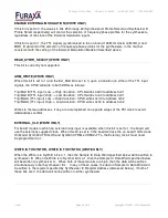
ENABLE EXTERNAL MODULATION (WRITE ONLY)

If this bit is set to 0, the values in bits 25 through 22 (Synthesizer A Profile Select and Synthesizer B
Profile Select respectively) will control the selection of frequency/phase profiles for the synthesizers,
regardless of the state of the External modulation inputs.

If this bit is set to 1, the TTL signals (synchronized to the on-board 125 MHz clock) on MOD_A and
MOD_B will control the selection of frequency/phase profiles for the synthesizers, in the manner
consistent with the setting of the External Modulation Mode bit described above.

READ_SYNTH_SELECT (WRITE ONLY)

This bit is currently not supported.

ARM_WRITE (WRITE ONLY)

When this bit is set to 1 (and the Ext_Mod bit is set to 1) upon a transition on either of the TTL input
signals, the CPLD will write to both DDSs as follows:

Trig/Mod B (TTL input) Low -> High transition:  CPLD writes 0x80 to address 0x01
Trig/Mod B (TTL input) High -> Low transition:  CPLD writes 0x00 to address 0x01
Trig/Mod A (TTL input) Low -> High transition:  CPLD writes 0xC0 to address 0x02
Trig/Mod A (TTL input) High -> Low transition:  CPLD writes 0x00 to address 0x02

Writes to the two addresses, if any, are accomplished on opposite edges of the PCI clock to avoid
data/address conflict.

EXTERNAL_CLK (WRITE ONLY)

For board models in which an external clock input is available, when this bit is set to 1, the board will
use the externally supplied clock.  When this bit is set to 0 the board will use the on board 1GHz clock.
On Model Synth300-TRIG-HS and Synth300-TRIG-TTL, the External_clk bit must never
be programmed to 1.

WRITE IS TO SYNTH B, WRITE IS TO SYNTH A (WRITE ONLY)

When the Write is to Synth B bit is a 1, then the Sample IC Data Word specified below will be written to
synthesizer B.  When the Write is to Synth A bit is a 1, then the Sample IC Data Word specified below
will be written to synthesizer A.   When both of these two bits are high, then the data will be written
simultaneously to both synthesizer ICs.   In any of these cases, the data in Sample IC Data Word will
be written to the register specified by Synthesizer IC Register Address (discussed below).  If both of
these bits are 0, the data will not be written to either synthesizer.

r1v06

Page 

29

 of 

31

Copyright © 2008 – 2010 Furaxa Inc.

Summary of Contents for SYNTH300-TRIG

Page 1: ...com Visit us at www furaxa com SYNTH300 TRIG SYNTH300 TRIG LVDSX2 And SYNTH300 TRIG HS Dual 100 kHz 300 MHz Direct Digital Synthesizer Covers Boards With Firmware rev 1 00 5 2 05 With software for Win...

Page 2: ...10 Ext Clk LED 10 ARM Sweep LED 10 Synth On LED 10 HARDWARE INSTALLATION AND SETUP 11 WINDOWS SOFTWARE INSTALLATION 12 Software Package Contents 12 The Example Program 12 Software Installation for Win...

Page 3: ...Update write only 28 Synthesizer A Profile Select write only 29 Synthesizer B Profile Select write only 29 External Modulation Mode write only 29 Enable External Modulation write only 30 Read_Synth_S...

Page 4: ...ted or error free Furaxa Inc products are not intended to be used as critical components in life support systems aircraft military systems or other systems whose failure to perform can reasonably be e...

Page 5: ...trol A single LVDS channel is supported on the LVDSB output connectors MODEL SYNTH300 TRIG OPTION LVDSX2 Model Synth300 TRIG LVDSX2 is a Dual channel DDS board with two independent Direct Digital Synt...

Page 6: ...1 MHz TBD 40MHz Fout 50 kHz TBD 100MHz Fout 1 MHz TBD 100MHz Fout 50 kHz TBD 180MHz Fout 1 MHz TBD 180MHz Fout 50 kHz TBD Output Phase Noise 103MHz Iout 1kHz Offset TBD 10kHz Offset TBD 100kHz Offset...

Page 7: ...utput lines 1 Standard TTL V0l 0 8V Vih 2 4V LVDSB AND LVDSB OUTPUTS Output connectors 2 SMA connectors Number of LVDS Output ports 1 Standard differential LVDS LVDS output driver type TI SN65LVDS100D...

Page 8: ...MHz PCI slots with either 5V or 3 3V signalling environment The figure below shows the locations of the SMA signal output and digital I O connectors and LED indicators To avoid overheating all SYNTH30...

Page 9: ...tput lines are driven by a TI SN65LVDS100DGK LVDS driver which receives the output generated by DDSB after filtering TRIG MODA AND TRIG MODB I O LINES The MODA and MODB jacks are used as profile selec...

Page 10: ...YNTH300 board that are useful during system integration for monitoring the board status The functions of the LEDs are outlined below EXT CLK LED For board models in which an external clock input is av...

Page 11: ...a mixture of 5V and 3 3V slots are available in the system choose a 32 bit 5V slot as your first preference If that is not available install it in a 32 or 64 bit 3 3V slot For details refer to the ha...

Page 12: ...information is contained in the C code comments SOFTWARE INSTALLATION FOR WINDOWS 2000 OR WINDOWS XP When you reboot your system for the first time with the Synth300 board properly installed you may s...

Page 13: ...e executed from anywhere on the user s hard disk to control the configuration and operation of the device RUNNING SYNTH300 PROGRAMS The GUI provided Synth300 GUI exe allows the user to specify each of...

Page 14: ...he current settings and resulting outputs The lower left hand portion allows selection of the Synth300 board to write to if multiple boards are installed in the system as well as check boxes for exter...

Page 15: ...1 TWO INDEPENDENT SINUSOIDS 123 000000 MHz is generated on Synth A and 220 000001MHz on Synth B Notice that Profile 0 is selected on each synthesizer by use of the bullets to the right of the frequen...

Page 16: ...IDS 5 000000 MHz is generated on Synth A and 5 000000MHz on Synth B with a 90 degree phase offset Profile 1 was used for both synthesizers while retaining the Profile 0 settings Each synthesizer has f...

Page 17: ...0 MHz from Synth A increasing at 1MHz sec Sweep Rate 1e 006 hz sec for 10 seconds Sweep Period 10 Sec Then repeating 10 000000MHz from Synth B decreasing Negative Sweep Checked at 1MHz sec Sweep Rate...

Page 18: ...ysical location of ModA and ModB input jacks If External Modulation is checked the TTL signals on Trigger Modulation Control A and Trigger Modulation Control B synchronized to the on board 125 MHz clo...

Page 19: ...the clock SMA 2 Connect an SMA cable from the SYNTH300 TRIG HS clock output to an external amplifier power splitter creating the necessary number of clocks of correct amplitude for the slave SYNTH300...

Page 20: ...mmer would modify this section as required SYNTH300 OPERATIONAL OVERVIEW The Synth300 device uses a combination of AD9858 DDS core implemented and firmware CPLD implemented functionality This combinat...

Page 21: ...bilities of a Synth300 device without the need to understand the low level software interface to the control registers on the Synth300 An explanation of the low level software interface is included in...

Page 22: ...date event is required for any function starting with Enter_ to take effect One method of generating a valid update event is through use of the Update function For futher information refer to the Upda...

Page 23: ...ep rate parameters to the corresponding DDS This is done by use of the Enter_Sweep_Rate function The first argument identifies which DDS is targeted FALSE SynthA TRUE SynthB The second and third argum...

Page 24: ...tion effectively acts as both the update event for the settings prior to the transition and the signal to prime the corresponding function frequency sweep enable disable or autoclear enable disable to...

Page 25: ..._clk BOOLEAN verbose_flag Gvien proper jumper configuration of the MODB output jack see figure 4 1 the user can select to output the 125 MHz clock or the SynthA output By setting TTL_125Select to TRUE...

Page 26: ...registers must be made as 32 bit transfers PCI CONFIGURATION HEADER SYNTH300 series boards support a PCI Configuration Header whose map is shown below Double Word Address byte 3 byte 2 byte 1 byte 0...

Page 27: ...re use 17 Arm_Write 16 External_Clk 15 Write is to Synth B 14 Write is to Synth A 13 8 Synthesizer IC register address 5 0 7 0 Synthesizer IC data word 7 0 Function of Control Register bits during wri...

Page 28: ...h the second bit controlled by software If external modulation is disabled this bit is ignored If External Modulation is enabled and this bit is set to a 0 the TTL signals synchronized to the on board...

Page 29: ...Low High transition CPLD writes 0xC0 to address 0x02 Trig Mod A TTL input High Low transition CPLD writes 0x00 to address 0x02 Writes to the two addresses if any are accomplished on opposite edges of...

Page 30: ...specified by the 8 bit data word Synthesizer IC Data Word 7 0 discussed below SAMPLE IC DATA WORD WRITE ONLY This 8 bit value is written to the register specified in IC Register Address 5 0 to the syn...

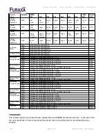
Page 31: ...ed 0x00 Frequency Tuning Word 1 0x10 Frequency Tuning Word for Profile_1 7 0 0x11 Frequency Tuning Word for Profile_1 15 8 0x12 Frequency Tuning Word for Profile_1 23 16 0x13 Frequency Tuning Word for...

Reviews: