


9
2. FUNCTIONAL DESCRIPTION
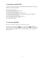
2.1 Transmission
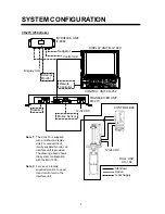
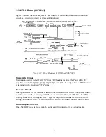
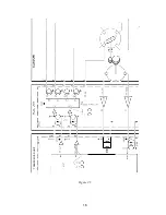
Fig. 2.1 shows the signal flow in the transmitter.
The TX signal, TX0 and TX1, generated by CPU board (06P0258) is amplified by TRX board
(06P0241). The output of the power amplifier is impedance-matched with the transducer with a
matching transformer on PRA board (06P0259).
The +B voltage (VTX) from PWR board (06P0242) determines the transmitter output level
according to menu settings.
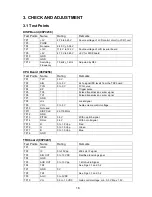
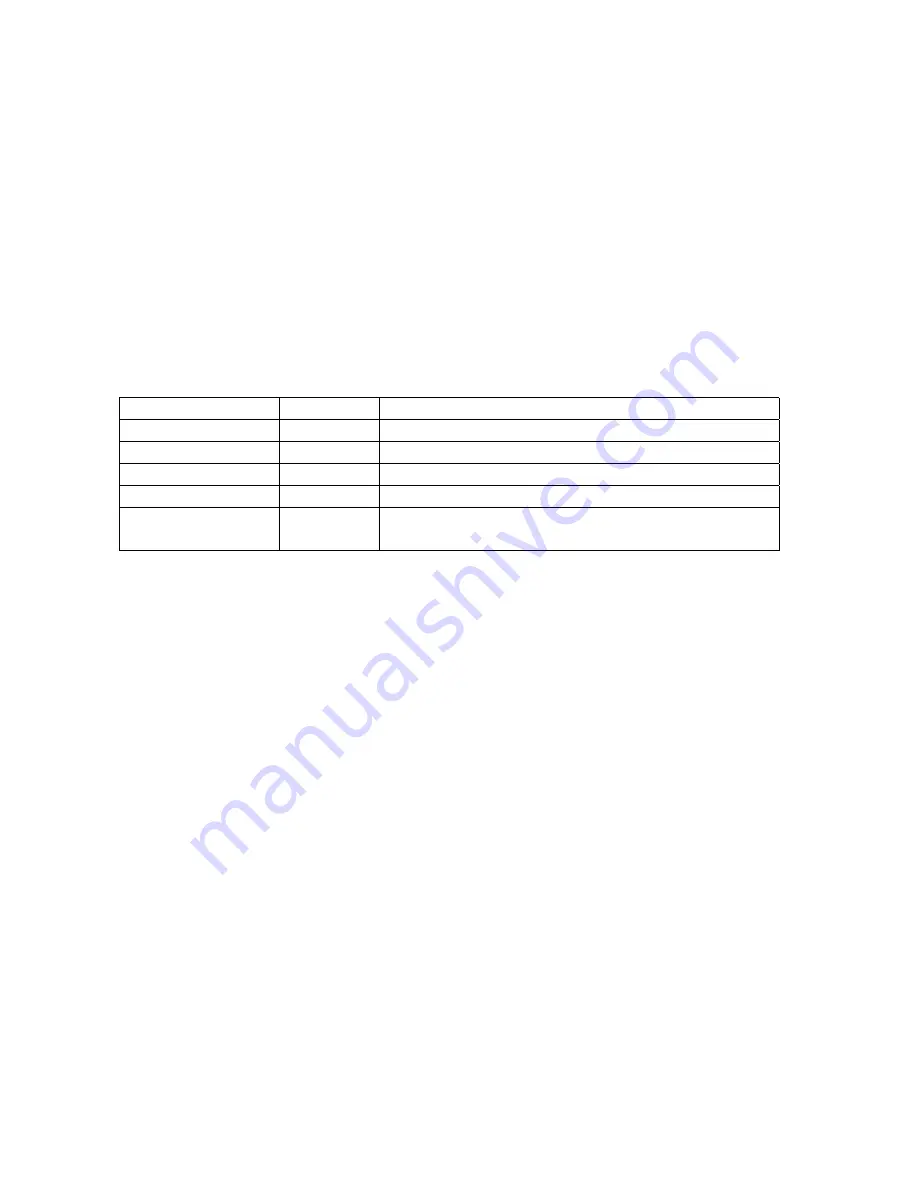
Table 2.1 Transmission level and control voltage
Signals Voltage
Measuring
Points
TX output
1019 Vpp
Output of matching transformer on PRA board
TX output
713 Vpp
Between TP6 and TP8 on TRX board
VTX (+B voltage)
77 V
Resister "R13" on TRX board
Control Voltage TXV
3.0 V
TP1 on CPU board
TX output level with
Dummy Load
592 Vpp
Between TP6 and TP8 on TRX board with Dummy Load
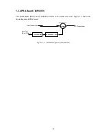
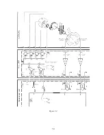
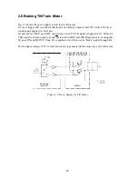
2.2 Reception
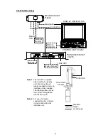
Fig. 2.2 shows the signal flow in the receiver.
The echo received by the transducer is amplified by the Pre-Amplifier board and mixed with the
local carrier signal by the mixer U2 to generate 455 kHz IF signal.
The output of the buffer amplifier Q5 is sent to the rectifier, CR8/CR9, and then output to CPU
board from J3 #1.
The gain control signal (TVG), 0 to 5 VDC, is generated by CPU board according to control
panel setting. The TVG/AGC control circuit reshapes the TVG signal and output TVG signal,
0.5 to 1.7 VDC to amplifiers. When GAIN control is set to maximum, 1.7VDC is output.
Receiving the signal rectified by U7, the AGC feedback circuit also controls the TVG signal
level.
The output of TRX board is converted into digital data by A/D converter "U35" and applied to
Gate Array "U30" on CPU board.
The output of Gate Array is converted into R/G/B signal and sent to the display unit from #1, #2,
and #3 of J1.
Summary of Contents for CH-270
Page 1: ...COLOR SEARCHLIGHT SONAR CH 270...
Page 13: ...10 58 59 6 6 DRV 06P0154 Hull Unit XDR Slip ring Figure 2 1 Signal Flow in Transmitter...
Page 14: ...11 Hull unit XDR Slip ring 6 6 59 58 Figure 2 2 Signal Flow in Receiver...
Page 19: ...16 Figure 2 5 TRANSCEIVER UNIT CPU J2 3 4 3 4 5 6 J10 5 6 7 8 CR16 U17 U34 191 R104 R105...
Page 23: ...20 DRV Board 06P0154...
Page 54: ......
Page 55: ......
Page 64: ......
Page 65: ......
Page 66: ......
Page 67: ......
Page 68: ......
Page 69: ......
Page 70: ......
Page 71: ......
Page 72: ......
Page 73: ......
Page 74: ......
Page 75: ......
Page 76: ......
Page 77: ......
Page 78: ......
Page 79: ......
Page 80: ......
Page 81: ......
Page 82: ......
Page 83: ......
Page 84: ......
Page 85: ......
Page 86: ......
Page 87: ......
Page 88: ......


