background image

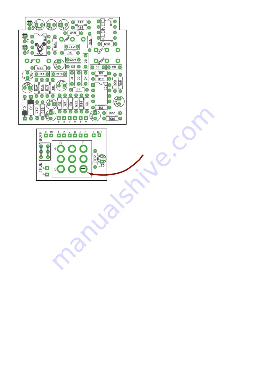
The Buffered/True-Bypass selection is

designed for a 2.54mm-pitch miniature slide

switch.
If you prefer to hardwire one way or the other,

wire in jumpers as shown above. Red for True

Bypass, blue for Buffered.
Anode (+) leg of electrolytic caps go into the

square pad.
Cathode (-) leg of diodes and the LED go into

the square pads.
Snap the little metal tag off the pots to mount

them flush in the box.
You should use some kind of heat sink on the

legs of the diodes when soldering. They aren’t

keen on heat. Any more than 3-4 seconds of

iron and they’re toast. Use sockets for the ICs

or be extra careful with them too.
Footswitch lugs should be horizontal and

inndicated above.
The current limiting resistor for the LED goes

into the spot marked ‘CLR’ on the

daughterboard. We supply 2K2.

Be VERY careful when bending the legs of the

germanium diodes. The glass case is very

fragile and likely to break. Hold the leg with

some needle-nosed pliers against the case,

and bend the leg with your finger so the

pliers are taking any strain away from it.

To give yourself more clearance when

mounting the circuit into your enclosure,

C17 and C20 can be bent over the adjacent

components as shown in the cover image.

Connect the two PCBs together using pads

1  2  V  G  3  4

Your jacks connect to G / IN and G / OUT on

the daughterboad.
DC connections are G and V pads next to

‘TRUE’.

PCB Layout ©2017 Pedal Parts Ltd.

PART SUBSTITUTIONS

The circuit benefits from some extra bass in

both the gain and clean sections:

C2

100n (clean)

C6

120 - 150n (gain)

The Tone (Treble) control has a more useful

range if you increase 

C14

to 6n8 or 8n2. 

Footswitch lugs should be horizontal

Summary of Contents for Klone V4

Page 1: ...Klone V4 Ultimate box of transparent overdrive Contents of this document are 2017 Pedal Parts Ltd No reproduction permitted without the express written permission of Pedal Parts Ltd All rights reserved ...

Page 2: ...wise stated in this document this circuit is designed to be powered with 9V DC COMPONENT SPECS Unless otherwise stated in this document Resistors should be 0 25W You can use those with higher ratings but check the physical size of them Electrolytics caps should be at least 25V for 9V circuits 35V for 18V circuits Again check physical size if using higher ratings LAYOUT CONVENTIONS Unless otherwise...

Page 3: ... 100n C2 68n C3 390n 330n IS FINE C4 100n C5 68n C6 82n C7 1u tant C8 390p C9 1u elec C10 1u elec C11 2n2 C12 27n C13 560p 820p C14 3n9 C15 4u7 elec C16 4u7 elec C17 47u elec C18 1u elec C19 1u elec C20 47u elec C21 1u elec C22 1u elec BOM is for Silver Pony version Gold version values shown in blue If using a 7660 for IC3 you need one with an S suffix This ensures it will operate at a frequency h...

Page 4: ...into the spot marked CLR on the daughterboard We supply 2K2 Be VERY careful when bending the legs of the germanium diodes The glass case is very fragile and likely to break Hold the leg with some needle nosed pliers against the case and bend the leg with your finger so the pliers are taking any strain away from it To give yourself more clearance when mounting the circuit into your enclosure C17 an...

Page 5: ...ht and check to see if the heights line up If not melt that soldered joint and adjust Once you re happy all the pots are aligned you can solder in the other legs Make sure you don t push the pot pins all the way into the PCB There s not a lot of clearance on the bottom of the dual gang so it has to sit a little way up from the PCB ...

Page 6: ...d avoid any potential whining issues associated with charge pumps do the following Leave out C18 C19 C21 C22 D4 D5 IC3 Place jumper wires in place of D4 D5 C19 No buffer If you prefer to keep things True Bypass and you want to use your own daughterboard you can get rid of the buffered bypass element Leave out R24 R26 R27 C16 Take wires from the following pads to your daughterboard or switch wiring...

Page 7: ...Wire it up switching board ...

Page 8: ...Wire it up true bypass ...

Page 9: ...t particularly elegant but pad 1 from the main board should connect directly to the footswitch lug as shown It should actually work fine without this wire but it follows the original in that it grounds the output of the gain section on bypass ...

Page 10: ...2 4 3 1 What s going on with those switches Here s what s connected to what Jack IN Jack OUT GND BUFFERED TRUE BYPASS ...

Page 11: ...ts Ltd can accept no responsibility for incorrect drilling of enclosures FuzzDog co uk Drilling template Hammond 1590B 60 x 111 x 31mm It s a good idea to drill the pot and toggle switch holes 1mm bigger if you re board mounting them Wiggle room good Recommended drill sizes Pots 7mm Jacks 10mm Footswitch 12mm DC Socket 12mm Toggle switch 6mm 22mm 32mm ...

Reviews: