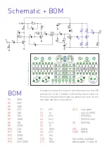
Sch BOM
BOM
R1
2M2
R2
22K
R3
1M2
R4
47K
R5
10K
R6
15K
R7
100K
R8
1M
R9
470K
R10
47K
R11
10K
R12
390R
R13
100K
R14
CLR (2K2)
C1
47n
C2
1n
C3
47n
C4
2n2
C5
3n3
C6
1n
C7
100n
C8
47n
C9
10u
C10
10u
C11
100u
Q1,2
Low gain
silicon NPN
(2N3904,
2N2222 etc)
Q3
2N3904
VOL
50KB
FUZZ
50KB
See notes overleaf
about pads J1 and J2.
Components shown in
blue
on the schematic are the LPB
post-boost circuit. To make it without the boost, leave out
the blue components and place a jumper wire across the
two pads marked in blue above.
PC
B
La
yo
ut
©
20
15
P
ed
al
P
ar
ts
L
td
.


