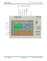
GS2011M Architecture
GS2011M Low Power WiFi Module Data Sheet
Wireless LAN and System Control Subsystem
24
Confidential
Preliminary
GS2011M-DS-001211, Release 0.9
At any time, any of these memory blocks can be assigned to one of the CPU subsystem.
These should be set up by the APP CPU SW at initialization time. The assignment is not
intended to change during operation and there is no HW interlock to avoid switching in the
middle of a memory transaction. The assignment to the WLAN CPU should be done
starting from the highest block number going down to lowest block number. This result in
the shared memory appearing as a single bank for each CPU subsystem, independent of the
number of blocks assigned. The shared memory is mapped such that the SRAM space is
continuous from the dedicated SRAM to shared SRAM.
A 64KB dual port memory is used for exchange of data between the two CPU domains.
Each CPU subsystem can read or write to this memory using an independent memory port.
SW must manage the memory access to avoid simultaneous write to the same memory
location. The dual port memory appears as a single bank to each CPU subsystem.
ROM
ROM is provided in each CPU subsystem to provide the boot code and other functional
code that are not expected to change regularly. Each CPU has 512KB of ROM.
OTP ROM
The GS2000 device includes a 64Kbit OTP ROM used for storing MAC ID and other
information such as security keys etc. The APP and WLAN subsystem each contain
32Kbits (4Kbytes) of OTP memory.
Flash Interface
The GS2000 SoC has only internal ROM and RAM for code storage. There is no embedded
Flash memory on the SoC. Any ROM patch code and new application code must reside in
the on-module Flash device of the GS2011M module. Flash access from the two CPUs are
independent. The APP CPU is considered the system Master and the code running on this
CPU is required to initialize the overall chip and common interfaces. WLAN CPU access
to the Flash is restricted to read DMA. Any write to the Flash from the WLAN CPU must
be done through the APP CPU. The operational parameters of the DMA accesses are set by
the APP CPU at system startup. The Flash code is transferred to internal RAM before
execution.
Clocks
The GS2011M includes four basic clock sources:
–
Low power 32KHz clock (see
Real Time Clock (RTC) Overview, page 25
)
–
40MHz Xtal Oscillator
–
PLL to generate the internal 120MHz (CPU) and 80MHz (PHY) clocks from the
40MHz Xtal.
–
High speed RC oscillator 80MHz


