GS2011M Low Power WiFi Module Data Sheet
Pin-out and Signal Description
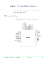
GS2011Mxx Device Pin-out
GS2011M-DS-001211, Release 0.9
Confidential Preliminary
39
20
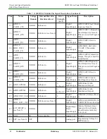
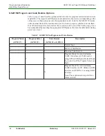
GPIO13/
SPI1_CS_n_1
VDDIO
Pull-down
4
Digital
Input/Output
GPIO/ Serial Peripheral
Interface 1 Chip Select_1
(Active Low)
21
GPIO21/
CLK_RTC
VDDIO
Pull-down
4
Digital
Input/Output
GPIO/Internal RTC Clock
Circuitry Test Point. This
pin is used for Code
Restore.
22
GPIO20/
CLK_HS_RC
VDDIO
Pull-down
4
Digital
Input/Output
GPIO/Internal RTC Clock
Circuitry Test Point
23
GPIO19/
CLK_HS_XTAL
VDDIO
Pull-down
4
Digital
Input/Output
GPIO/XTAL Clock
Circuitry Test Point
24 GPIO10/PWM0
VDDIO
Pull-down
4
Digital
Input/Output
GPIO/XTAL Clock
Circuitry Test Point
25 GPIO9/I2C_CLK VDDIO
Pull-down (see Note 4)12
Digital
Input/Output
GPIO/Inter-Integrated
Circuit Clock
26 GPIO8/I2C_DATA VDDIO
Pull-down (see Note 4)12
Digital
Input/Output
GPIO/Inter-Integrated
Circuit Data
27
GPIO36/
SDIO_DAT0/
SPI0_DOUT
VDDIO
Pull-down (see Note 1)4
Digital
Input/Output
GPIO/SDIO Data Bit0/SPI0
Transmit Data Output to the
HOST
28
GPIO35/
SDIO_CLK/
SPI0_CLK
VDDIO
Pull-down (see Note 1)4
Digital
Input/Output
GPIO/SDIO Clock/SPI0
Clock Input from the HOST
29
GPIO33/
SDIO_DAT3/
SPI0_CS_n_0
VDDIO
Pull-up (see Note 1)
4
Digital Input
Output
GPIO/SDIO Data Bit
3/SPI0 Chip Select Input 0
from the HOST (Active
Low)
30
GPIO34/
SDIO_CMD/
SPI0_DIN
VDDIO
Pull-down (see Note 1)4
Digital
Input/Output
GPIO/SDIO Command
Input/SPI0 Receive Data
Input from HOST
31 VIN_3V3
VIN_3V3 Not Applicable
Analog port
Single Supply Port
32 GND
0V
Not Applicable
Analog port
Ground
33 EN_1V8
VDDIO
Need to be driven
HIGH or LOW
Digital Input
Internal 1.8V regulator
enable port Active High
34 VDDIO
VDDIO
Not Applicable
Analog port
All I/O voltage domain (can
be tied to VIN_3V3 or tied
to HOST I/O supply)
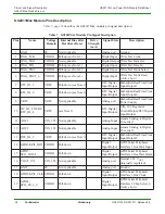
Table 7 GS2011Mxx Module Pin Signal Description (Continued)
Pins
Name
Voltage
Domain
Internal Bias after
Hardware Reset
Drive
Strength
(mA)
Signal State
Description

