background image


- 2 -


DX 949


CHAPTER 1


SPECIFICATIONS 


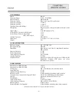
1.0 GENERAL


Model DX 

949 

Frequency Range 

26.965 - 27.405MHz. 

Emission Modes 

AM/USB/LSB 

Frequency Control 

Phase Lock Loop (PLL) synthesizer. 

Frequency Tolerance 

±

 0.005 %. 

Frequency Stability 

±

 0.001 %. 

Operating Temperature Range 

-30

°

C to +50

°

C. 

Microphone 

Plug-in dynamic; with push-to-talk switch and coiled 
cord. 

Input Voltage 

13.8V DC nominal 

±

15%. 

Current Drain : Transmit (AM full mod.) 

<3.5A. 

Current Drain : Receiver (Squelched) 

<0.5A. 

                                       (Max. audio output) 

<1.0A. 

Antenna Connector 

UHF, SO239. 

Dimensions 

2-3/8”(H) x 7-7/8”(W) x 9-1/4”(D). 

Weight 5 

lb. 


1.1 TRANSMITTER


RF Power Output 

AM : 4W SSB : 12W  

RF Transmit Modes 

AM/SSB  

Modulation  

High and low level Class B, Amplitude Modulation : 
AM and SSB   

Spurious Emissions 

-55 dB. 

Carrier Suppression 

-55 dB. 

Audio Frequency Response 

300 to 2500Hz    

Antenna Impedance  

50 Ohms. 

Output Indicators 

Meter shows relative RF output power, SWR and AM 
Modulation. Transmit LED glows red when 
transmitter is in operation.  


1.2 RECEIVER


Sensitivity For 10dB S/N (AM) 

<0.5

µ

Sensitivity For 10dB S/N (SSB) 

<0.25

µ

V.  

IF Frequency  

AM : 10.695 MHz 1st IF, 455 KHz 2nd IF. 

Image Rejection  

-65 dB. 

Adjacent Channel Selectivity 

-60 dB. 

RF Gain Control  

45 dB adjustable for optimum signal reception. 

Automatic Gain Control (AGC) Figure Of Merit 

100 mV for 10 dB Change in Audio Output 

Squelch 

Adjustable; threshold less than 0.5 

µ

V. 

Noise Blanker  

RF type. 

Audio Output Power 

2 watts into 8 Ohms. 

Audio Frequency Response 

AM and SSB : 300 to 2500 Hz. 

Built-in Speaker 

8 Ohms, round. 

External Speaker (Not Supplied) 

8 Ohms; disables internal speaker when connected. 


(SPECIFICATIONS SUBJECT TO CHANGE WITHOUT NOTICE) 

Summary of Contents for DX 949

Page 1: ......

Page 2: ...stallation 8 CHAPTER 3 CIRCUIT DESCRIPTION 3 0 Introduction 11 3 1 PLL Circuit 11 3 2 Receiver Circuit 11 3 3 Transmitter Modulation Circuit 11 3 4 Transmitter Amplifier Circuit 11 CHAPTER 4 ALIGNMENT...

Page 3: ...us Emissions 55 dB Carrier Suppression 55 dB Audio Frequency Response 300 to 2500Hz Antenna Impedance 50 Ohms Output Indicators Meter shows relative RF output power SWR and AM Modulation Transmit LED...

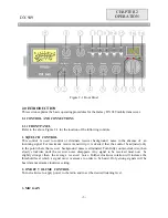
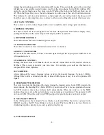
Page 4: ...or maximum receiver sensitivity it is desired that the control be adjusted only to the point where the receiver background noise is eliminated Turn fully counter clockwise then slowly clockwise until...

Page 5: ...onitor signal strength RF output power SWR level and AM modulation level 9 TALKBACK CONTROL Pushing this knob turns the Talkback circuit on and off Adjust this knob for desired volume of Talkback This...

Page 6: ...t have much effect on the signal to noise ratio of strong signals It is mostly used for SSB reception 14 MODE SWITCH This control allows you to select one of the following operating modes USB AM LSB 1...

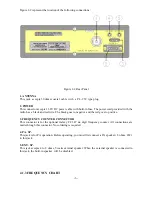
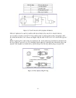
Page 7: ...to negative and the red goes to positive 3 FREQUENCY COUNTER CONNECTOR This connector is for the optional Galaxy FC 347 six digit frequency counter All connections are made through this connector No...

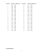
Page 8: ...65 MHz 7 27 035 MHz 27 27 275 MHz 8 27 055 MHz 28 27 285 MHz 9 27 065 MHz 29 27 295 MHz 10 27 075 MHz 30 27 305 MHz 11 27 085 MHz 31 27 315 MHz 12 27 105 MHz 32 27 325 MHz 13 27 115 MHz 33 27 335 MHz...

Page 9: ...control at this setting This SQ is now properly adjusted The receiver will remain quiet until a signal is actually received Do not advance the control too far or some of weaker signals will not be hea...

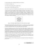
Page 10: ...d the plastic insulating jacket of the microphone cable ii All leads should be cut to the same length Strip the ends of each wire 1 8 and tin the exposed wire Before beginning the actual wiring read c...

Page 11: ...hed back onto the microphone cable before starting to solder If the washer is not captive to the pin receptacle body make sure that it is placed on the threaded portion of the pin receptacle body befo...

Page 12: ...sisting of Q17 The RF signal is fed into the mixer circuit of the Q18 and then into the AM IF section of the receiver depending on the mode of operation The signal is then detected by either the AM de...

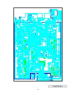
Page 13: ...12 DX 949 CIRCUIT DIAGRAM...

Page 14: ...13 CHAPTER 4...

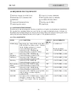
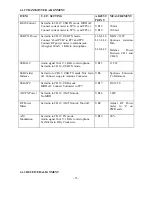
Page 15: ...e short PCB from TP7 TP8 and TP9 Set radio to CH 1 AM RX mode Clarifier setting in 12 o clock Connect Oscilloscope to TP3 Set radio to CH 1 AM RX mode Connect frequency counter IC 3 Pin 8 L14 L15 VC1...

Page 16: ...nce Power Between CH 1 and CH 40 SSB ALC Audio signal 30 mV 1 KHz to microphone Set radio to CH 19 USB TX mode VR13 11 5 W SSB Carrier Balance Set radio to CH 19 USB TX mode Mic Gain off Connect scope...

Page 17: ...y clockwise RF SG setting to 27 184 MHz 0 5 uV MOD to off L11 L12 Audio output 2V S N 10 dB NB Adjust Set radio to CH 19 AM mode RF SG setting 27 205 MHz 100 uV MOD 30 NB ANL switch on Connect Voltmet...

Page 18: ...17 Figure 4 2 Receiver test setup...

Page 19: ...18 Figure 4 3 Main PCB Adjustment Locations CHAPTER 5...

Page 20: ...t periodic inspection and maintenance Important points to be checked regularly are as follows Check Item Action Whip antenna option If cracked or broken replace it Coaxial cable If sheath is cracked s...

Page 21: ...e parts list The reference designators are in alphanumeric order PART LIST DX 949 VR P C B ITEM REFERENCE NUMBER RANGER PART NUMBER DESCRIPTION 1 EPT095950Z VR P C B 2 J1 J2 EX07N48223 PCB C S 2P 3 J3...

Page 22: ...RCY012224Z 2 2K ohm 0 1W 8 R12 RCY014724Z 4 7K ohm 0 1W 9 R7 RCY011034Z 10K ohm 0 1W 10 C5 RCY012234Z 22K ohm 0 1W 10 C7 CK1059AB1A 0 5PF 50V 11 C6 CK1030AB1A 3PF 50V 12 C3 C4 CK2104AB7R 0 1 F 50V 13...

Page 23: ...22...

Page 24: ...712G TR 2SC2712 4 ROTARY SW EWRT32000S ROTARY SW 5 J7 J9 J10 EX07N48223 PCB C S 2P 6 J1 EX07N48234 PCB C S 2P 7 J3 J5 EX07N48350 PCB C S 3P 8 J4 EX07W48824 PCB C S 3P 9 J6 EX07N48490 PCB C S 4P 10 J2...

Page 25: ...1 EPT690050Z MIC P C B 2 C501 C502 C503 C504 CC0501027L 0 001 F 50V 3 C505 C506 CC0501037L 0 01 F 50V 4 Q501 TDTA0124ES T R DTA124ES 5 L501 ECCHK16001 CHOKE COIL 5 6 H 6 L502 ECBAD18526 BEAD COIL 7 MI...

Page 26: ...m 1 4W 5 C3 RCU141024Z 1K ohm 1 4W 6 R3 RCU144724Z 4 7K ohm 1 4W 7 R2 RCU141034Z 10K ohm 1 4W 8 R8 RCM144724B 4 7K ohm 1 4W 9 R10 WX01070712 JUMPER WIRE 10 C4 C5 C6 CC0501037L 0 01 F 50V 11 C2 CE02510...

Page 27: ...GAIN RV10203528 VR 1KB 4 DIM ON OFF RV50203542 5KB PUSH SW 5 MIC R B ON RV10203541 1KA PUSH SW 6 RF POWER RV50203525 VR 5KB 7 BAND P C B ENRG0IC080 MODULAR IC080 8 JP1 WX01070710 JUMPER WIRE 9 J2 J8 J...

Page 28: ...SPLAY 3 R325 R326 RCY011024Z 1K ohm 0 1W 4 C501 CK1103AB6U 0 01 F 50V 5 ANT EX01Y40116 LED LAMP 6 R B EX01Y40117 LED LAMP 7 T R EX01Y40114 LED LAMP 8 HI MED LO EWSL31027K SLIDE SW 9 USB AM LSB EWSL310...

Page 29: ...28 DX 949 MAIN PCB REMARK SOLDER SIDE WHITE...

Page 30: ...4 RCP161064Z 10M 1 16W R244 RCP121514Z 150 1 2W R239 RCP121034Z 10K 1 2W C218 CC0500301L 3PF 50WV C79 CC0500501L 5PF 50WV C1 49 108 147 CC0501004L 10PF 50WV C76 CC0501804L 18PF 50WV C36 CC0502704L 27P...

Page 31: ...7 5tmm L35 ECSPG18001 0 8x3 5x7t L38 ECRFZ10048 25UH L39 41 13 ECBAD18526 3 5x6x1 2 VR7 12 16 18 RE10200041 1K VM6CK PV VR13 14 RE50200042 5K VM6CK PV VR1 2 6 17 RE10300031 10K VM6CK PV VR9 15 RE10400...

Page 32: ...31 IC8 ENTA07222A TA7222AP Q54 T2SB00754Y 2SB754Y Q49 T2SC02166C 2SC2133C Q47 T2SC01969C 2SC1969C Q37 T2SA01869Z 2SA1869...

Page 33: ...32...

Page 34: ...33 AT0949040A...

Page 35: ...34...

Reviews: