background image


GS66508B-EVBDB1 

 650V GaN E-HEMT Evaluation Board User’s Guide 

___________________________________________________________________________________________________________________ 

GS66508B-EVBDB1 UG rev. 190605 

© 2019 GaN Systems Inc.    

www.gansystems.com                          11 


Please refer to the Evaluation Board/Kit Important Notice on page 30 


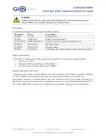
WARNING 

ALWAYS double check the jumper setting and PWM gate drive signals before applying power. 
Incorrect PWM inputs or jumper settings may cause device failures  


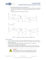
Test points


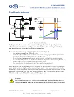
Test points are designed in groups/pairs to facilitate probing: 

Test points 

Name 

Description 

TP1/TP2 

+5V/0V 

5V bias power 

TP7/TP8 

PWMIN/0V 

PWM input signal from J7 

TP4/TP3/TP13 

PWMH/PWML/0V 

High/low side gate signals to daughter board 

TP9/TP10 

VDC+/VDC- 

DC bus voltage 

TP11/TP12 

VOUT/VDC- 

Output voltage  

TP6/TP5 

VSW/VDC- 

Switching node output voltage (for HV oscilloscope probe) 


Power connections


CON1-CON7 mounting pads are designed to be compatible with following mounting terminals: 


#10-32 Screw mount, 


Banana Jack PCB mount (Keystone P/N: 

575-4

), or 


PC Mount Screw Terminal (Keystone P/N: 

8191


Output passives (L and C14) 

An external power inductor (not included) can be connected between VSW (CON1) and VOUT (CON4/5) 
or VDC+ (CON2/3) for double pulse test. Users can choose their inductor size to meet the test 
requirement. Generally it is recommended to use power inductor with low inter-winding capacitance to 
obtain best switching performance. For the double pulse testing we use 2x 60uH/40Amp inductor (CWS, 
P/N: HF467-600M-40AV) in series. C14 is designed to accommodate a film capacitor as output filter. 


Summary of Contents for GS66508B-EVBDB1

Page 1: ...for the latest version of this user s guide DANGER This evaluation kit is designed for engineering evaluation in a controlled lab environment and should be handled by qualified personnel ONLY High vo...

Page 2: ...ching characterization testing Universal form factor and footprint for all products The daughter board and universal mother board ordering part numbers are below Table 1 Ordering part numbers Part Num...

Page 3: ...9 GaN Systems Inc www gansystems com 3 Please refer to the Evaluation Board Kit Important Notice on page 30 Power pins The 3 power pins are VDC Input DC Bus voltage VSW Switching node output VDC Input...

Page 4: ...08B 30A 50m B Decoupling capacitors C4 C11 C 2 x Analog Devices ADuM4121ARZ Isolated gate driver D Optional current shunt position JP1 E Test points for bottom Q2 VGS F Recommended probing positions f...

Page 5: ...l times of approximately 18 ns The very high Common mode transient immunity CMTI of 150 kV us min isolates high transient noise during the high frequency operation and prevents erroneous outputs The G...

Page 6: ...d supply 9V at VDRV Figure 6 Gate drive power supply with optional bootstrap mode Current shunt JP1 The board provides an optional current shunt position JP1 between the source of Q2 and power ground...

Page 7: ...ent shunt 1 When measuring VSW with current shunt ensure all channel probe grounds and current shunt BNC output case are all referenced to the source end of Q2 before the current shunt The recommended...

Page 8: ...evaluation kit includes a sample 35x35mm fin heatsink not installed although other heatsinks can also be used to fit users system design 3 A thermal tape type TIM Berguist Bond Ply 100 is chosen for i...

Page 9: ...VB GaN Systems offers a universal 650V mother board ordering part number GS665MB EVB sold separately that can be used as the basic evaluation platform for all the daughter boards The universal 650V mo...

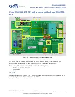
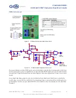
Page 10: ...PWM signals non inverted and inverted controlled by J7 input with dead time or external high low side drive signals from J5 users own control board An on board dead time generation circuit is include...

Page 11: ...low side gate signals to daughter board TP9 TP10 VDC VDC DC bus voltage TP11 TP12 VOUT VDC Output voltage TP6 TP5 VSW VDC Switching node output voltage for HV oscilloscope probe Power connections CON...

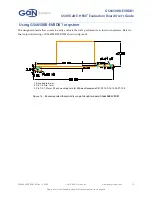
Page 12: ...the Evaluation Board Kit Important Notice on page 30 Using GS66508B EVBDB1 in system The daughter board allows users to easily evaluate the GaN performance in their own systems Refer to the footprint...

Page 13: ...current starts to ramp up until t1 The period of first pulse Ton1 defines the switching current ISW VDS TON1 L 3 t1 t2 is the free wheeling period when the inductor current IL forces Q1 to conduct in...

Page 14: ...6 VSW CON5 COUT RLoad This is standard half bridge configuration that can be used in following circuits Synchronous Buck DC DC Single phase half bridge inverter ZVS half bridge LLC Phase leg for full...

Page 15: ...nect PWM input gate signal 0 5V to J7 If it is generated from a signal generator ensure the output mode is high Z mode c Set J4 to OFF position and J7 to INT d Set High voltage HV DC supply voltage to...

Page 16: ...________________________________________________________________________________________ GS66508B EVBDB1 UG rev 190605 2019 GaN Systems Inc www gansystems com 16 Please refer to the Evaluation Board K...

Page 17: ...rising drain current di dt in the power loop V Lpxdi dt where Lp is the total power loop inductance After the drain current reaches the inductor current the Vds starts to fall The Vgs undershoot spike...

Page 18: ..._____________________________________ GS66508B EVBDB1 UG rev 190605 2019 GaN Systems Inc www gansystems com 18 Please refer to the Evaluation Board Kit Important Notice on page 30 Figure 17 Double pul...

Page 19: ...ent shunt SDN 414 10 0 1 is installed for switching loss measurement as shown below Figure 1917 Eon Eoff measurement probe connection with current shunt Figure 2018 Eon Eoff measurement and test bench...

Page 20: ...____________________________________________________ GS66508B EVBDB1 UG rev 190605 2019 GaN Systems Inc www gansystems com 20 Please refer to the Evaluation Board Kit Important Notice on page 30 Figur...

Page 21: ...dominates the overall hard switching loss Eon at 0A is the Qoss loss caused by the Coss at high side switch The turn off loss remain almost constant from 0A up to 20A about 8uJ the measured Eoff match...

Page 22: ..._______________________________________________________________________________________________ GS66508B EVBDB1 UG rev 190605 2019 GaN Systems Inc www gansystems com 22 Please refer to the Evaluation...

Page 23: ..._______________________________________________________________________________________ GS66508B EVBDB1 UG rev 190605 2019 GaN Systems Inc www gansystems com 23 Please refer to the Evaluation Board Ki...

Page 24: ...________________________________________________________________________________________________ GS66508B EVBDB1 UG rev 190605 2019 GaN Systems Inc www gansystems com 24 Please refer to the Evaluation...

Page 25: ...______________________________________________________________________________________________________________ GS66508B EVBDB1 UG rev 190605 2019 GaN Systems Inc www gansystems com 25 Please refer to...

Page 26: ...____________________________________________________________________________________________________ GS66508B EVBDB1 UG rev 190605 2019 GaN Systems Inc www gansystems com 26 Please refer to the Evalua...

Page 27: ...R R1206 R2 100R R1206 U2A 74VHC132 3 1 2 14 7 0V R1 49R9 0V D2 PMEG2005EB SOD523 VDC TR2 2K C12 100pF 0V U2B 74VHC132 4 5 6 U2C 74VHC132 9 10 8 U2D 74VHC132 12 13 11 VDC CON5 1 CON7 1 TP3 TP4 TP1 TP2...

Page 28: ...______________________________________________________________________________________________ GS66508B EVBDB1 UG rev 190605 2019 GaN Systems Inc www gansystems com 28 Please refer to the Evaluation B...

Page 29: ...M BLOCK HDR 2POS R A 5 08MM CON TERM BLK 2POS RA TE CONNECTIVITY 796638 2 11 1 J1 PLUG TERM BLOCK BLUG 2POS 5 08MM TE CONNECTIVITY 796634 2 12 1 J2 CONN RCPT 6POS 100 DBL STR PCB CON RCPT 2X3 BOT HARW...

Page 30: ...kit may be returned within 30 days from the date of delivery for a full refund THE FOREGOING WARRANTY IS THE EXCLUSIVE WARRANTY MADE BY THE SELLER TO BUYER AND IS IN LIEU OF ALL OTHER WARRANTIES EXPRE...

Page 31: ...re not designed authorized or warranted for use in lifesaving life sustaining military aircraft or space applications nor in products or systems where failure or malfunction may result in personal inj...

Reviews: