Installation Procedures
2-22
560-0982-01 Rev A
GNS 480 (CNX80) Installation Manual
2.7.1.4 Nav I/O Connector (P7)
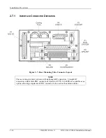
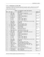
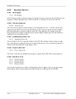
A navigation I/O connector, which handles VHF NAV / GPS switching, resolver and main CDI/VDI
interfaces, is located vertically on the left side of the rear panel. The NAV I/O hooks internally to the
VHF NAV board and consists a standard 37-pin D-sub connector, and has a pinout similar to the SL30
VHF NAV unit for simpler field upgrading. The pinout for the connector is defined in the following
table.
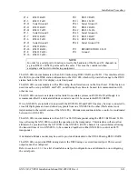
Table 2-8 NAV I/O Connector Pin-Out (P7)
Pin #
I/O
Name
Description
Reference
1
I
Power +
Main Aircraft Power Input (+10 to +36 VDC)
2.8.1
2
I
Power ground
Main Aircraft Power Ground
3
O
Spare ground
No current assignment
4 --
RESERVED
RESERVED
5
--
RESERVED DB30 TxD
RESERVED (for use with the DB30)
2.8.10.1
6 --
RESERVED
RESERVED
7
I
OBS_ D {S1}
OBS Resolver input pin from channel D (COS)
2.8.2
8
I
Main CDI Select In
Selects between GPS & VHF NAV on Main CDI Output
2.8.9.1
9
O
Main GS Superflag
Glideslope Indicator Valid flag output (high-level )
2.8.2
10
O
Main CDI + Valid
Nav Valid flag output (low-level)
11
O
Main CDI + FROM
+ From flag output
12
O
Main CDI + TO
+ To flag output
13
O
Main CDI + Right
CDI + Right output
14
O
Main CDI + Left
CDI + Left output
15
O
Back Course Out
active low output when reverse sensing is engaged
2.8.7.2
16
O
OBS_ F {S4}
OBS OBS Resolver input pin from channel F (SIN)
2.8.2
17
O
GPS Indicator Out
active low output when GPS selected on Main CDI output 2.8.7.1
18
O
NAV Indicator Out
active low output when VHF NAV selected on Main CDI
out
19
O
Composite Out
VOR/LOC composite signal
2.8.4
20
O
NAV Audio Ground
audio signal ground pin
2.8.13.1
21 --
RESERVED
RESERVED
22 --
RESERVED
RESERVED
23
O
NAV Audio Out
low-level nav audio output
2.8.13.1
24
O
OBS_H {R HI}
OBS Resolver output pin to channel H
2.8.2
25
O
OBS_C {R LO}
OBS Resolver return signals C
26
I
OBS_E {S3}
OBS Resolver return signals E
27
O
Main CDI Superflag
CDI high-level Valid flag output
28
O
Main GS + Valid
Nav Valid flag output (low-level )
29
O
Main CDI - Valid
Nav Valid flag signal ground
30
O
Main GS + Up
Glid Up output
31
O
Main GS + Down
Glid Down output
32
O
Main GS - Valid
Glideslope Valid flag signal ground
33
O
ILS Energize
active low output when a localizer frequency is tuned
2.8.8.1
34
O
OBS_G {S2}
OBS Resolver return signals G
2.8.2
35 --
RESERVED
RESERVED
36
O
Power Control Out
power control output sinks up to 50ma when unit is on
2.8.8.4
37
O
Composite Ground
return path for the composite signal
2.8.4
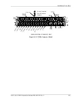
(see Figure 2-8 for a diagram of a 37-pin connector)
Summary of Contents for GNS 480
Page 1: ...GNS 480 CNX80 Color GPS Nav Com Installation Manual September 2004 560 0982 01 Rev A...
Page 10: ...Table of Contents viii 560 0982 01 Rev A GNS 480 CNX80 Installation Manual NOTES...
Page 30: ...General Information 1 20 560 0982 01 Rev A GNS 480 CNX80 Installation Manual NOTES...
Page 126: ...Periodic Maintenance 6 2 560 0982 01 Rev A GNS 480 CNX80 Installation Manual NOTES...
Page 150: ...Appendix D Interconnect Diagrams D 2 560 0982 01 Rev A GNS 480 CNX80 Installation Manual NOTES...
Page 185: ......
Page 186: ......


