background image

1–172

345 TRANSFORMER PROTECTION SYSTEM – COMMUNICATIONS GUIDE

MODBUS FUNCTIONS

CHAPTER 1: COMMUNICATIONS GUIDE

For the 345 implementation of Modbus, this function code can be used to read any actual 
values (“input registers”). Input registers are 16 bit (two byte) values transmitted high order 
byte first. Thus all 345 Actual Values are sent as two bytes. The maximum number of 
registers that can be read in one transmission is 125.
The slave response to this function code is the slave address, function code, a count of the 
data bytes to follow, the data itself and the CRC. Each data item is sent as a two byte 
number with the high order byte sent first. 
For example, request slave 17 to respond with 1 register starting at address 0008. For this 
example the value in this register (0008) is 0000. 

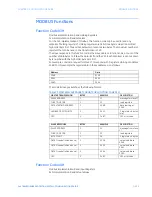
Table 34: MASTER/SLAVE PACKET FORMAT FOR FUNCTION CODE 04H

Function Code 05H

Modbus Implementation: Force Single Coil
345 Implementation: Execute Operation
This function code allows the master to request a 345 to perform specific command 
operations.
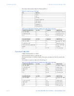
For example, to request slave 17 to execute operation code 1 (reset), we have the following 
master/slave packet format:

Table 35: MASTER/SLAVE PACKET FORMAT FOR FUNCTION CODE 05H

 MASTER TRANSMISSION

 BYTES

 EXAMPLE

 DESCRIPTION

 SLAVE ADDRESS

 1

 11

 message for slave 17

 FUNCTION CODE

 1

 04

 read registers

 DATA STARTING ADDRESS

 2

 00 08

 data starting at 0008

 NUMBER OF ACTUAL VALUES

 2

 00 01

 1 register = 2 bytes

 CRC

 2

 B2 98

 CRC error code

 SLAVE RESPONSE

 BYTES

 EXAMPLE

 DESCRIPTION

 SLAVE ADDRESS

 1

 11

 message from slave 

17

 FUNCTION CODE

 1

 04

 read registers

 BYTE COUNT

 1

 02

 1 register = 2 bytes

 DATA (see definition above)

 2

 00 00

 value in address 

0008

 CRC

 2

 78 F3

 CRC error code

 MASTER TRANSMISSION

 BYTES

 EXAMPLE

 DESCRIPTION

 SLAVE ADDRESS

 1

 11

 message for slave 17

 FUNCTION CODE

 1

 05

 execute operation

 OPERATION CODE

 2

 00 01

 operation code 1

 CODE VALUE

 2

 FF 00

 perform function

 CRC

 2

 DF 6A

 CRC error code

 SLAVE RESPONSE

 BYTES

 EXAMPLE

 DESCRIPTION

 SLAVE ADDRESS

 1

 11

 message from slave 

17

 FUNCTION CODE

 1

 05

 execute operation

 OPERATION CODE

 2

 00 01

 operation code 1

 CODE VALUE

 2

 FF 00

 perform function

 CRC

 2

 DF 6A

 CRC error code

Summary of Contents for 345

Page 1: ...ilin 215 Anderson Avenue Markham Ontario Canada L6E 1B3 Tel 905 294 6222 Fax 905 201 2098 Internet http www GEmultilin com Communications Guide SR345 revision 1 30 Manual P N 1601 9099 A1 GE publication code GEK 113570 Copyright 2010 GE Multilin 1601 xxxx A3 345 Transformer Protection System Transformer protection and control ...

Page 2: ...hpad and EnerVista SR3 Setup are registered trademarks of GE Multilin Inc The contents of this manual are the property of GE Multilin Inc This documentation is furnished on license and may not be reproduced in whole or in part without the permission of GE Multilin The content of this manual is for informational use only and is subject to change without notice Part number 1601 9099 A1 February 2010...

Page 3: ...s of ASDU 17 Selection of standard information numbers in monitor direction 17 Selection of standard information numbers in control direction 20 Basic application functions 20 Miscellaneous 21 Application level 21 Application functions 21 Type identification 21 Function type 22 Information number 22 Data management 22 Digital states 23 Measurands 23 Commands 24 103 general settings 25 Ethernet int...

Page 4: ...ture 68 GOOSE remote inputs 69 USB interface 72 MODBUS Protocol 72 Data Frame Format and Data Rate 72 Data Packet Format 72 Error Checking 73 CRC 16 Algorithm 73 Timing 74 345 supported functions 74 MODBUS memory map 75 Format Codes 128 MODBUS Functions 171 Function Code 03H 171 Function Code 04H 171 Function Code 05H 172 Function Code 06H 173 Function Code 07H 173 Function Code 08H 174 Function C...

Page 5: ...NICATIONS GUIDE 1 1 345 Transformer Protection System Communications Guide Digital Energy Multilin CommunicationsGuide Communications interfaces The 345 has three communications interfaces These can be used simultaneously RS485 USB Ethernet ...

Page 6: ...uld be connected to all of the 345s as well as the master then grounded at one location only This keeps the ground potential at the same level for all of the devices on the serial link NOTE NOTE Polarity is important in RS485 communications The positive terminals of every device must be connected together MODBUS Protocol The 345 implements a subset of the Modicon Modbus RTU serial communication st...

Page 7: ...s includes a two byte CRC 16 16 bit cyclic redundancy check with every transmission The CRC 16 algorithm essentially treats the entire data stream data bits only start stop and parity ignored as one continuous binary number This number is first shifted left 16 bits and then divided by a characteristic polynomial 11000000000000101B The 16 bit remainder of the division is appended to the end of the ...

Page 8: ...Data packet synchronization is maintained by timing constraints The receiving device must measure the time between the reception of characters If 3 5 character times elapse without a new character or completion of the packet then the communication link must be reset i e all slaves start listening for a new transmission from the master Thus at 9600 baud a delay of greater than 3 5 x 1 9600 x 10 x x...

Page 9: ... 2 PORT TME SYNC IIN PER DNP MSG FRAG SIZE DNP TCP CONN T O S1 DNP DNP GENERAL DNP UNSOL RESPONSE DEFAULT VARIATION DNP CLIENT ADDRESS DNP POINTS LIST 897769 cdr DNP CLIENT ADDRESS CLIENT ADDRESS 1 CLIENT ADDRESS 2 CLIENT ADDRESS 3 CLIENT ADDRESS 4 CLIENT ADDRESS 5 POINT 0 POINT 1 POINT 2 POINT 63 S1 DNP POINTS LIST BINARY INPUTS BINARY OUTPUT ANALOG INPUTS POINT 0 ENTRY POINT 1 ENTRY POINT 31 ENT...

Page 10: ...ject 1 Binary Input Changes Object 2 Binary Outputs Object 10 Control Relay Output Block Object 12 Binary Counters Object 20 Frozen Counters Object 21 Counter Change Event Object 22 Frozen Counter Event Object 23 Analog Inputs Object 30 Analog Input Changes Object 32 Analog Deadbands Object 34 Time and Date Object 50 Internal Indications Object 80 Maximum Data Link Frame Size octets Maximum Applic...

Page 11: ...ays Sometimes Configurable Pulse On Never Always Sometimes Configurable Pulse Off Never Always Sometimes Configurable Latch On Never Always Sometimes Configurable Latch Off Never Always Sometimes Configurable Queue Never Always Sometimes Configurable Clear Queue Never Always Sometimes Configurable Explanation of Sometimes Object 12 points are mapped to Virtual Inputs Both Pulse On and Latch On ope...

Page 12: ...ation 0 is used to request default variation 1 read 22 assign class 00 01 start stop 06 no range or all 07 08 limited quantity 17 28 index 1 Binary Input 1 read 22 assign class 00 01 start stop 06 no range or all 07 08 limited quantity 17 28 index 129 response 00 01 start stop 17 28 index see Note 2 2 Binary Input with Status 1 read 22 assign class 00 01 start stop 06 no range or all 07 08 limited...

Page 13: ...k 9 freezeclear 10 frz cl noack 22 assign class 00 01 start stop 06 no range or all 07 08 limited quantity 17 28 index 129 response 00 01 start stop 17 28 index see Note 2 5 32 Bit Binary Counter without Flag 1 read 7 freeze 8 freeze noack 9 freezeclear 10 frz cl noack 22 assign class 00 01 start stop 06 no range or all 07 08 limited quantity 17 28 index 129 response 00 01 start stop 17 28 index s...

Page 14: ...sol resp 17 28 index 5 32 Bit Counter Change Event with Time 1 read 06 no range or all 07 08 limited quantity 129 response 130 unsol resp 17 28 index 6 16 Bit Counter Change Event with Time 1 read 06 no range or all 07 08 limited quantity 129 response 130 unsol resp 17 28 index 0 Frozen Counter Event Variation 0 is used to request default variation 1 read 06 no range or all 07 08 limited quantity ...

Page 15: ...o range or all 07 08 limited quantity 129 response 130 unsol resp 17 28 index 2 16 Bit Analog Change Event without Time 1 read 06 no range or all 07 08 limited quantity 129 response 130 unsol resp 17 28 index 3 32 Bit Analog Change Event with Time 1 read 06 no range or all 07 08 limited quantity 129 response 130 unsol resp 17 28 index 4 16 Bit Analog Change Event with Time 1 read 06 no range or al...

Page 16: ...0 01 start stop 07 08 limited quantity 17 28 index 50 1 Time and Date default see Note 1 1 read 2 write 00 01 start stop 06 no range or all 07 limited qty 1 08 limited quantity 17 28 index 129 response 00 01 start stop 17 28 index see Note 2 52 2 Time Delay Fine quantity 1 129 response 07 limited quantity 60 0 Class 0 1 2 and 3 Data 1 read 20 enable unsol 21 disable unsol 22 assign class 06 no ran...

Page 17: ... Even F102 Rear 485 Protocol DNP 3 0 Modbus IEC60870 5 103 DNP 3 0 F97 SETTINGS PARAMETER RANGE FORMAT DNP Unsol Resp Function Disabled Disabled Enabled F126 DNP Unsol Resp Timeout 5 s 0 to 60 s F1 DNP Unsol Resp Max Retries 10 1 to 255 F1 DNP Unsol Resp Dest Addr 1 0 to 65519 F1 DNP Time Sync IIN Period 1440 min 1 to 10080 min F1 DNP Message Fragment Size 240 30 to 2048 F1 DNP Object 1 Default Va...

Page 18: ... Inputs and Commands Force Coils Some legacy DNP implementations use a mapping of one DNP Binary Output to two physical or virtual control points In Order to configure Paired Control Points the source for states ON and OFF should be set to different Virtual Inputs or Commands The DNP Technical Committee recommends using contiguous point numbers starting at 0 for each data type because some DNP3 Ma...

Page 19: ...nges by more than its configured deadband limit There can be up to 3 Masters in total but only one Serial Master The following Default Classes will be fixed for the different blocks of data Binary Input Points Default Class 1 Analog Input Point Default Class 2 Counters Default Class 3 Each Data Point Class can be changed by protocol function code 22 in volatile mode If a restart is performed the n...

Page 20: ...ENERAL SLAVE ADDRESS SYNCH TIMEOUT 897770 cdr S1 103 MEASURANDS FIRST ASDU SECOND ASDU THIRD ASDU FOURTH ASDU S1 60870 5 103 GENERAL BINARY INPUTS MEASURANDS COMMANDS S1 103 COMMANDS CMD 0 FUNC TYPE CMD 0 INFO NO CMD 0 ON OPER CMD 0 OFF OPER CMD 15 FUNC TYPE CMD 15 INFO NO CMD 15 ON OPER CMD 15 OFF OPER S1 103 FOURTH ASDU ID TYPE FUNCTION TYPE INFORMATION NO SCAN TIMEOUT FIRST ANLG ENTRY FIRST ANL...

Page 21: ...t is used exclusively in this companion standard Common address of ASDU Selection of standard information numbers in monitor direction Table 5 System functions in monitor direction Glass fibre Plastic fibre F SMA type connector BFOC 2 5 type connector 9600 bits s 19200 bits s One COMMON ADDRESS OF ASDU identical with station address More than one COMMON ADDRESS OF ASDU INF Semantics 0 End of gener...

Page 22: ...rameter setting 23 Characteristic 1 24 Characteristic 2 25 Characteristic 3 26 Characteristic 4 27 Auxiliary input 1 28 Auxiliary input 2 29 Auxiliary input 3 30 Auxiliary input 4 INF Semantics 345 Identifier 345 Data Text 32 Measurand supervision I 33 Measurand supervision V 35 Phase sequence supervision 36 Trip circuit supervision 37 I back up operation 38 VT fuse failure 39 Teleprotection distu...

Page 23: ... back up operation 73 Fault location X in ohms 74 Fault forward line 75 Fault reverse busbar 76 Teleprotection signal transmitted 77 Teleprotection signal received 78 Zone 1 79 Zone 2 80 Zone 3 81 Zone 4 82 Zone 5 83 Zone 6 84 General start pick up 85 Breaker failure 86 Trip measuring system L1 87 Trip measuring system L2 88 Trip measuring system L3 89 Trip measuring system E 90 Trip I 91 Trip I 9...

Page 24: ...f generic data 249 Write entry with confirmation 250 Write entry with execution 251 Write entry aborted INF Semantics 0 Initiation of general interrogation 0 Time synchronization INF Semantics 16 Auto recloser on off 17 Teleprotection on off 18 Protection on off 19 LED reset 23 Activate characteristic 1 24 Activate characteristic 2 25 Activate characteristic 3 26 Activate characteristic 4 INF Sema...

Page 25: ... the complete database The measurands will be sent to the primary station as a response to class 2 request A setting 0 to 60 min is available to configure the desired interval where 0 means transmission as fast as possible The following functions are supported Initialization General Interrogation Synchronization Commands transmission Type identification The Type Identification implemented will be ...

Page 26: ...ol as overcurrent protection so it will use the Function Type 160 for all the digital and analogues points proposed by the standard and mapped in this profile For the other data supported by the device the customer will have the capability to use them by setting a number from the private range Information number INFORMATION NUMBER UI8 1 8 0 255 Monitor direction 0 255 0 15 system functions 16 31 s...

Page 27: ... been identified in the device profile For the other measurands it is possible to use the EnerVista SR3 Setup to select the desired point and assign the Identification Type 3 or 9 Function Type 0 255 and Information Number 1 255 If the user selects Identification Type 3 ASDU 3 only four measurands are available for configuration but if Identification Type 9 ASDU 9 is selected up to nine measurands...

Page 28: ... program It is possible to choose the desired command for the ON state and the same or different command for the OFF state The user is able to select the Information Number 1 255 and the Function Type 0 255 command mappings but the Identification Type 20 General Commands is fixed There are 32 configurable commands In this case it will be necessary to define a new format For example FC500 Modbus Ad...

Page 29: ...d bit will be set in the time stamp of a time tagged message It is necessary to configure other port settings Baud Rate etc Description Value Virtual Input 1 0 Virtual Input 2 1 Virtual Input 32 31 Reset 32 Open 35 Close 36 Modbus Address Description Value Format Command 1 Function Type 0 255 F1 Command 1 Information Number 0 255 F1 Command 1 Operation ON 2 FC500 Command 1 Operation OFF 8 FC500 Co...

Page 30: ...alues are obtained and averaged it generally takes 10 seconds until the clock is synchronized with the SNTP server It may take up to 30 seconds for the device to signal an SNTP FAIL state if the server is off line In this case the main CPU generates an alarm similar to that of the IRIG B case To use SNTP in broadcast mode set the function setting to BROADCAST The device listens to SNTP messages se...

Page 31: ...s only a subset of the MODBUS protocol functions Data and control functions The following functions are supported 01H Read Coil Status Just respond no action required for now Outgoing message for this function is the same as input one 02H Read Input Status Just respond no action required for now Outgoing message for this function is the same as input one 03H Read Holding Registers Reads the binary...

Page 32: ...the binary contents right justified within each byte For each register the first byte contains the high order bits and the second contains the low order bits 05H Force Single Coil Forces a single coil 0X reference to either ON or OFF The query message specifies the coil reference to be forced Coils are addressed starting at zero coil 1 is addressed as 0 The reguested ON OFF state is specified by a...

Page 33: ...tual Input 23 0x1016 Virtual Input 8 0x1007 Virtual Input 24 0x1017 Virtual Input 9 0x1008 Virtual Input 25 0x1018 Virtual Input 10 0x1009 Virtual Input 26 0x1019 Virtual Input 11 0x100A Virtual Input 27 0x101A Virtual Input 12 0x100B Virtual Input 28 0x101B Virtual Input 13 0x100C Virtual Input 29 0x101C Virtual Input 14 0x100D Virtual Input 30 0x101D Virtual Input 15 0x100E Virtual Input 31 0x10...

Page 34: ...On 56 eCmdCO13_Off 57 eCmdCO14_On 58 eCmdCO14_Off 59 eCmdCO15_On 60 eCmdCO15_Off 61 eCmdCO16_On 62 eCmdCO16_Off 63 eCmdCO17_On 64 eCmdCO17_Off 65 eCmdCO18_On 66 eCmdCO18_Off 67 eCmdCO19_On 68 eCmdCO19_Off 69 eCmdCO20_On 70 eCmdCO20_Off 71 eCmdCO21_On 72 eCmdCO21_Off 73 eCmdCO22_On 74 eCmdCO22_Off 75 eCmdCO23_On 76 eCmdCO23_Off 77 eCmdCO24_On 78 eCmdCO24_Off 79 eCmdCO25_On 80 eCmdCO25_Off 81 eCmdCO...

Page 35: ...TDMaximums 112 eCmdResetMotorInfo 113 eCmdAutoMode 114 eCmdManualMode 115 eCmdManualInhibit 116 eCmdManualRestore 117 eCmdStartInhibit 118 eCmdStartRestore 119 eCmdTriggerWaveform 120 eCmdStartDataLog 121 eCmdStopDatalog 122 eCmdTempResetIntValues 123 eCmdTempFactoryClear 124 eCmdTempFactoryStoreSample 125 eCmdClearSecurityLog 126 eCmdStartUploadingSetpointFile 127 eCmdEndUploadingSetpointFile 128...

Page 36: ... 161 eCmdReloadFactorySetpts1 162 eCmdSecurityMin 163 eCmdFactoryUse1 164 eCmdFactoryUse2 165 eCmdFactoryUse3 166 eCmdFactoryUse4 167 eCmdFactoryUse5 168 eCmdFactoryUse6 169 eCmdFactoryUse7 170 eCmdFactoryUse8 171 eCmdFactoryUse9 172 eCmdFactoryUse10 173 eCmdPaintGCPRed 174 eCmdPaintGCPGreen 175 eCmdPaintGCPBlue 176 eCmdReboot2 177 eCmdReboot1 178 eCmdMAC2 179 eCmdMAC1 180 eCmdCalOffsets2 181 Fiel...

Page 37: ...for this function is the same as input one 16 10 Hex Preset Multiple Registers Presets values into a sequence of holding registers 4X references Query The query message specifies the register references to be preset Registers are addressed starting at zero register 1 is addressed as 0 The requested preset values are specified in the query data field Data is packed as two bytes per register Here is...

Page 38: ...is function number is used to read the settings for each group Example Field Name Hex Slave Address FE Function 10 Starting Address Hi 0F Starting Address Lo 0A No of Registers Hi 00 No of Registers Lo 02 Byte Count 04 04 Data Hi 00 Data Lo 01 Data Hi 00 Data Lo 00 Field Name Hex Slave Address FE Function 10 Starting Address Hi 0F Starting Address Lo 0A No of Registers Hi 00 No of Registers Lo 02 ...

Page 39: ...at high bit rates Modbus protocol can be implemented at any standard communication speed The SR350supports operation at 9600 19200 38400 57600 and 115200 baud Request response sequence A complete request response sequence consists of the following bytes transmitted as separate data frames Master Request Transmission SLAVE ADDRESS 1 byte FUNCTION CODE 1 byte DATA variable number of bytes depending ...

Page 40: ...eristic polynomial 11000000000000101B The 16 bit remainder of the division is appended to the end of the transmission MSByte first The resulting message including CRC when divided by the same polynomial at the receiver will give a zero remainder if no transmission errors have occurred If a 345 Modbus slave device receives a transmission in which an error is indicated by the CRC 16 calculation the ...

Page 41: ...345 TRANSFORMER PROTECTION SYSTEM COMMUNICATIONS GUIDE 1 37 The algorithm is 1 FFFF hex A 2 0 i 3 0 j 4 Di AL AL 5 j 1 j 6 shr A 7 is there a carry No go to 8 Yes G A A 8 is j 8 No go to 5 Yes go to 9 9 i 1 i 10 is i N No go to 3 Yes go to 11 11 A CRC ...

Page 42: ...T O S1 DNP DNP GENERAL DNP UNSOL RESPONSE DEFAULT VARIATION DNP CLIENT ADDRESS DNP POINTS LIST 897769 cdr DNP CLIENT ADDRESS CLIENT ADDRESS 1 CLIENT ADDRESS 2 CLIENT ADDRESS 3 CLIENT ADDRESS 4 CLIENT ADDRESS 5 POINT 0 POINT 1 POINT 2 POINT 63 S1 DNP POINTS LIST BINARY INPUTS BINARY OUTPUT ANALOG INPUTS POINT 0 ENTRY POINT 1 ENTRY POINT 31 ENTRY POINT 0 ON POINT 0 OFF POINT 1 ON POINT 1 OFF POINT 1...

Page 43: ...unters Object 21 Counter Change Event Object 22 Frozen Counter Event Object 23 Analog Inputs Object 30 Analog Input Changes Object 32 Analog Deadbands Object 34 Time and Date Object 50 Internal Indications Object 80 Maximum Data Link Frame Size octets Maximum Application Fragment Size octets Transmitted 292 Transmitted configurable up to 2048 Received 292 Received 2048 Maximum Data Link Re tries M...

Page 44: ...urable Latch Off Never Always Sometimes Configurable Queue Never Always Sometimes Configurable Clear Queue Never Always Sometimes Configurable Explanation of Sometimes Object 12 points are mapped to Virtual Inputs Both Pulse On and Latch On operations perform the same function in the 345 that is the appropriate Virtual Input is put into the On state The On Off times and Count value are ignored Pul...

Page 45: ...Counters Reported Configurable attach explanation Configurable attach explanation Default Object 20 16 Bits Default Variation 1 Point by point list attached Other Value _____ Point by point list attached Sends Multi Fragment Responses Yes No DNP 3 0 Device Profile Channel 1 Port Channel 2 Port DNP Availability None None DNP not available over Ethernet port None NETWORK TCP One Master over TCP None...

Page 46: ... read 06 no range or all 07 08 limited quantity 1 Binary Input Change without Time 1 read 06 no range or all 07 08 limited quantity 129 response 130 unsol resp 17 28 index 2 Binary Input Change with Time 1 read 06 no range or all 07 08 limited quantity 129 response 130 unsol resp 17 28 index 3 Binary Input Change with Relative Time 1 read 06 no range or all 07 08 limited quantity 10 0 Binary Outpu...

Page 47: ...29 response 00 01 start stop 17 28 index see Note 2 21 0 Frozen Counter Variation 0 is used to request defaultvariation 1 read 22 assign class 00 01 start stop 06 no range or all 07 08 limited quantity 17 28 index 1 32 Bit Frozen Counter 1 read 22 assign class 00 01 start stop 06 no range or all 07 08 limited quantity 17 28 index 129 response 00 01 start stop 17 28 index see Note 2 2 16 Bit Frozen...

Page 48: ...ad 06 no range or all 07 08 limited quantity 129 response 130 unsol resp 17 28 index 6 16 Bit Frozen Counter Event with Time 1 read 06 no range or all 07 08 limited quantity 129 response 130 unsol resp 17 28 index 30 0 Analog Input Variation 0 is used to request default variation 1 read 22 assign class 00 01 start stop 06 no range or all 07 08 limited quantity 17 28 index 1 32 Bit Analog Input 1 r...

Page 49: ... all 07 08 limited quantity 17 28 index 1 16 bit Analog Input Reporting Deadband default see Note 1 1 read 00 01 start stop 06 no range or all 07 08 limited quantity 17 28 index 129 response 00 01 start stop 17 28 index see Note 2 2 write 00 01 start stop 07 08 limited quantity 17 28 index 2 32 bit Analog Input Reporting Deadband 1 read 00 01 start stop 06 no range or all 07 08 limited quantity 17...

Page 50: ... or 08 will be responded with qualifiers 00 or 01 for changeevent objects qualifiers 17 or 28 are always responded 3 Cold restarts are implemented the same as warm restarts the 345 is not restarted but the DNP process is restarted 2 Class 1 Data 1 read 20 enable unsol 06 no range or all 07 08 limited quantity 3 Class 2 Data 21 disable unsol 4 Class 3 Data 22 assign class 80 1 Internal Indications ...

Page 51: ...ess 1 0 0 0 0 F150 DNP Client Address 2 0 0 0 0 F150 DNP Client Address 3 0 0 0 0 F150 DNP Client Address 4 0 0 0 0 F150 DNP Client Address 5 0 0 0 0 F150 DNP TCP UDP Port Number 20000 0 to 65535 F1 DNP Unsol Resp Function Disabled Disabled Enabled F126 DNP Unsol Resp Timeout 5 s 0 to 60 s F1 DNP Unsol Resp Max Retries 10 1 to 255 F1 DNP Unsol Resp Dest Addr 1 0 to 65519 F1 DNP Time Sync IIN Perio...

Page 52: ... to two physical or virtual control points In Order to configure Paired Control Points the source for states ON and OFF should be set to different Virtual Inputs or Commands The DNP Technical Committee recommends using contiguous point numbers starting at 0 for each data type because some DNP3 Master implementations allocate contiguous memory from point 0 to the last number for each data type NOTE...

Page 53: ...it There can be up to 3 Masters in total but only one Serial Master The following Default Classes will be fixed for the different blocks of data Binary Input Points Default Class 1 Analog Input Point Default Class 2 Counters Default Class 3 Each Data Point Class can be changed by protocol function code 22 in volatile mode If a restart is performed the new values will be lost DNP Object 34 points c...

Page 54: ...ignificant octet first as defined in Clause 4 10 of IEC 60870 5 4 is used exclusively in this companion standard 4 Common address of ADSU Two octets 5 Information object address Three octets Structured Unstructured 6 Cause of transmission 104 BINARY INPUTS POINT 0 POINT 1 POINT 63 S1 104 GENERAL FUNCTION CYCLIC DATA PERIOD TCP CONN TIMEOUT TCP PORT SLAVE ADDRESS 897794 cdr S1 104 POINT LIST BINARY...

Page 55: ...lue scaled value M_ME_NB_1 13 Measured value short floating point value M_ME_NC_1 15 Integrated totals M_IT_NA_1 20 Packed single point information with status change detection M_SP_NA_1 21 Measured value normalized value without quantity descriptor M_ME_ND_1 30 Single point information with time tag CP56Time2a M_SP_TB_1 31 Double point information with time tag CP56Time2a M_DP_TB_1 32 Step positi...

Page 56: ...aled value with time tag CP56Time2a C_SE_TB_1 63 Set point command short floating point value with time tag CP56Time2a C_SE_TC_1 64 Bitstring of 32 bits with time tag CP56Time2a C_BO_TA_1 Number description Mnemonic 70 End of initialization M_EI_NA_1 Number description Mnemonic 100 Interrogation command C_IC_NA_1 101 Counter interrogation command C_CI_NA_1 102 Read command C_RD_NA_1 103 Clock sync...

Page 57: ...an 3 Spontaneous 4 Initialized 5 Request or requested 6 Activation 7 Activation confirmation 8 Deactivation 9 Deactivation confirmation 10 Activation termination 11 Return information caused by local command 12 File transfer 13 Interrogated by group number 20 to 36 Requested by group n counter request 37 to 41 Unknown type identification 44 Unknown cause of transmission 45 Unknown command address ...

Page 58: ...1 40 M_EP_TF_1 45 C_SC_NA_1 46 C_DC_NA_1 47 C_RC_NA_1 48 C_SE_NA_1 49 C_SE_NB_1 50 C_SE_NC_1 51 C_BO_NA_1 58 C_SC_TA_1 59 C_DC_TA_1 60 C_RC_TA_1 61 C_SE_TA_1 62 C_SE_TB_1 63 C_SE_TC_1 64 C_BO_TA_1 70 M_EI_NA_1 100 C_IC_NA_1 101 C_CI_NA_1 102 C_RD_NA_1 103 C_CS_NA_1 104 C_TS_NA_1 105 C_RP_NA_1 106 C_CD_NA_1 107 C_TS_TA_1 110 P_ME_NA_1 111 P_ME_NB_1 112 P_ME_NC_1 113 P_AC_NA_1 120 F_FR_NA_1 Type ide...

Page 59: ...specific list Single point information M_SP_NA_1 M_SP_TA_1 M_SP_TB_1 and M_PS_NA_1 Double point information M_DP_NA_1 M_DP_TA_1 and M_DP_TB_1 Step position information M_ST_NA_1 M_ST_TA_1 and M_ST_TB_1 Bitstring of 32 bits M_BO_NA_1 M_BO_TA_1 and M_BO_TB_1 if defined for a specific project Measured value normalized value M_ME_NA_1 M_ME_TA_1 M_ME_ND_1 and M_ME_TD_1 Measured value scaled value M_ME_...

Page 60: ...ximum delay in command direction of commands and setpoint commands Maximum allowable delay of commands and setpoint commands 5 s 18 Transmission of integrated totals Mode A Local freeze with spontaneous transmission Mode B Local freeze with counter interrogation Mode C Freeze and transmit by counter interrogation commands Mode D Freeze by counter interrogation command frozen values reported simult...

Page 61: ...official Internet Standard which describes the state of standardization of protocols used in the Internet as determined by the Internet Architecture Board IAB It offers a broad spectrum of actual standards used in the Internet The suitable selection of documents from RFC 2200 defined in this standard for given projects has to be chosen by the user of this standard Ethernet 802 3 Serial X 21 interf...

Page 62: ...but are very useful for integrating the relay into a system By default the Object Information Address for the different data will be as follows M_SP Single Points 1000 M_ME Measured Value 2000 M_IT Integrated Totals 3000 C_SC or C_DC Single or Double Command 4000 IEC 60870 5 104 point lists The Single Points M_SP can be configured to a maximum of 64 points The value for each point is user programm...

Page 63: ...iod is configured to send the measurands to the Master The final way is to send the measurands spontaneously when a deadband overflow takes place Groups of Data The data will be organized in groups in order to provide values when the controlling station requests by general or group interrogation Group 1 will be set by the 64 Single Points M_SP Group 2 will be set by the 32 Measured values M_ME The...

Page 64: ...DBUS MODBUS MODBUS Settings Ethernet DNP CHANNEL 1 PORT TCP DNP CHANNEL 2 PORT NONE 104 GENERAL FUNCTION DISABLE Client 1 Client 2 Client 3 DNP NOTHING NOTHING DNP MODBUS NOTHING DNP MODBUS MODBUS Settings Ethernet DNP CHANNEL 1 PORT UDP DNP CHANNEL 2 PORT NONE 104 GENERAL FUNCTION DISABLE Client 1 Client 2 Client 3 Client 4 DNP NOTHING NOTHING NOTHING DNP MODBUS NOTHING NOTHING DNP MODBUS MODBUS ...

Page 65: ... 1 PORT TCP DNP CHANNEL 2 PORT UDP 104 GENERAL FUNCTION DISABLE Client 1 Client 2 Client 3 Client 4 DNP TCP DNP UDP NOTHING NOTHING DNP TCP DNP UDP MODBUS NOTHING DNP TCP DNP UDP MODBUS MODBUS Settings Ethernet DNP CHANNEL 1 PORT XX any value DNP CHANNEL 2 PORT XX any value 104 GENERAL FUNCTION ENABLE Client 1 Client 2 Client 3 IEC104 IEC104 NOTHING IEC104 IEC104 MODBUS ...

Page 66: ...n and reception settings for the GOOSE feature are performed using EnerVista SR3 Setup Software The 345 firmware accepts GOOSE messages from UR F650 and UR Plus The interoperability with other manufacturers will be guaranteed in almost all cases by implementing the reception side with nested structures one level of nesting and all the standard data types GOOSE settings changes will take effect onl...

Page 67: ...CHAPTER 1 COMMUNICATIONS GUIDE ETHERNET INTERFACE 345 TRANSFORMER PROTECTION SYSTEM COMMUNICATIONS GUIDE 1 63 ...

Page 68: ... a fixed value ON or OFF For GOOSE transmission the firmware allows users to assign through EnerVista SR3 Setup Software an DataSetReference composed as follows 1 IEDNameLDInst LLN0 2 the string default GOOSE1 contained in the Modbus address The IEDName is taken from setting S1 Relay Setup Installation Relay Name Setting the IEDName to Feeder_25Kv_Line1 for example would result in a DataSet Refere...

Page 69: ... mapped by the user to any available digital value within the 345 relay including Alarm elements Protection elements Pickup Dropout and Operate of all available protection elements Control element all available control elements Status of digital inputs Status of digital outputs Status of virtual inputs Status of virtual outputs The destination multicast address for GOOSE messages is composed of th...

Page 70: ...thin the specified amount of time GOOSE Status is also set to 0 if the next message is not accepted within the specified amount of time If a GOOSE message is received and its header has not been configured for reception the firmware ignores the message It is possible to see this GOOSE status information from the 345 relay front panel Data Item SR3 Text MMI Text Value Format Code Size in word s Mod...

Page 71: ...e level of nesting and that are capable of mapping only digital values to the remote inputs The 345 firmware maintains the format of GOOSE messages that can be received in MODBUS registers Configuration of GOOSE messages to be received by the device is implemented using the EnerVista SR3 Setup software as shown below either by reading in and parsing the ICD or SCD file from a remote device or by m...

Page 72: ...tal size of all Rx structures doesn t exceed the defined limit of 250 registers The User can configure the Datasets of his choice and if he exceeds the 250 registers limit when he tries to SAVE the following message appears saying that the selection of the user has exceeded the limit of 250 registers and that anything beyond will be lost Clicking on YES will save Dataset items selection up to 250 ...

Page 73: ... in a data set configured for reception to one of 32 GOOSE remote inputs More than 1 GOOSE remote input can be mapped to the same data element in a data set belonging to a received GOOSE message GOOSE remote inputs can only be mapped to digital data elements The firmware considers a GOOSE remote input to be in the on off state when the digital data element to which it is mapped is in the on off st...

Page 74: ...1 70 345 TRANSFORMER PROTECTION SYSTEM COMMUNICATIONS GUIDE ETHERNET INTERFACE CHAPTER 1 COMMUNICATIONS GUIDE Figure 6 EnerVista SR3 GOOSE Remote Inputs 1 Figure 7 EnerVista SR3 GOOSE Remote Inputs 2 ...

Page 75: ...le or multiple block setting group setting change user assignable LED digital output The 345 records changes in GOOSE remote inputs in the Event Log The time recorded in a GOOSE remote input s event log entry is the time at which the change in the input s state is detected The 345 invokes a logic block control function when its corresponding GOOSE remote input is asserted In the 345 there are many...

Page 76: ...onsists of 1 start bit 8 data bits and 1 stop bit This produces a 10 bit data frame This is important for transmission through modems at high bit rates Modbus protocol can be implemented at any standard communication speed The 345 supports operation at 9600 19200 38400 57600 and 115200 baud Data Packet Format A complete request response sequence consists of the following bytes transmitted as separ...

Page 77: ...one or more bytes of the transmission were received incorrectly and thus the entire transmission should be ignored in order to avoid the 345 performing any incorrect operation The CRC 16 calculation is an industry standard method used for error detection An algorithm is included here to assist programmers in situations where no standard CRC 16 calculation routines are available CRC 16 Algorithm On...

Page 78: ...on link must be reset i e all slaves start listening for a new transmission from the master Thus at 9600 baud a delay of greater than 3 5 x 1 9600 x 10 x x 3 65 x ms will cause the communication link to be reset 345 supported functions The following functions are supported by the 345 FUNCTION CODE 03 Read Setpoints FUNCTION CODE 04 Read Actual Values FUNCTION CODE 05 Execute Operation FUNCTION COD...

Page 79: ... 0xFFFF 1 F3 0 30135 86 Main Boot Code Date 0 6 1 F22 23 30141 8C Main Boot Code Time 0 4 1 F22 23 30145 90 Comm Boot Code Date 0 6 1 F22 23 30151 96 Comm Boot Code Time 0 4 1 F22 23 LAST TRIP DATA 30186 B9 Cause of Last Trip 0 59 1 FC134 0 REAL TIME CLOCK 30223 DE Weekday 0 7 1 None 0 30224 DF Date Read Only 0x010107D9 0x0C1F0833 0 F18 0x010107D9 30226 E1 Time Read Only 0 0X173B3B63 0 F19 0 30228...

Page 80: ...lt Cause 0 0xFFFFFFFF 1 FC188 0 USER MAP ACTUAL VALUES 30524 20B User Map Value 1 0 0xFFFF 1 F1 0 30525 20C User Map Value 2 0 0xFFFF 1 F1 0 30526 20D User Map Value 3 0 0xFFFF 1 F1 0 30527 20E User Map Value 4 0 0xFFFF 1 F1 0 30528 20F User Map Value 5 0 0xFFFF 1 F1 0 30529 210 User Map Value 6 0 0xFFFF 1 F1 0 30530 211 User Map Value 7 0 0xFFFF 1 F1 0 30531 212 User Map Value 8 0 0xFFFF 1 F1 0 3...

Page 81: ...ap Value 43 0 0xFFFF 1 F1 0 30567 236 User Map Value 44 0 0xFFFF 1 F1 0 30568 237 User Map Value 45 0 0xFFFF 1 F1 0 30569 238 User Map Value 46 0 0xFFFF 1 F1 0 30570 239 User Map Value 47 0 0xFFFF 1 F1 0 30571 23A User Map Value 48 0 0xFFFF 1 F1 0 30572 23B User Map Value 49 0 0xFFFF 1 F1 0 30573 23C User Map Value 50 0 0xFFFF 1 F1 0 30574 23D User Map Value 51 0 0xFFFF 1 F1 0 30575 23E User Map V...

Page 82: ... 89 0 0xFFFF 1 F1 0 30613 264 User Map Value 90 0 0xFFFF 1 F1 0 30614 265 User Map Value 91 0 0xFFFF 1 F1 0 30615 266 User Map Value 92 0 0xFFFF 1 F1 0 30616 267 User Map Value 93 0 0xFFFF 1 F1 0 30617 268 User Map Value 94 0 0xFFFF 1 F1 0 30618 269 User Map Value 95 0 0xFFFF 1 F1 0 30619 26A User Map Value 96 0 0xFFFF 1 F1 0 30620 26B User Map Value 97 0 0xFFFF 1 F1 0 30621 26C User Map Value 98 ...

Page 83: ...8 Date 0x010107D8 0X0C1F082E 0 F18 0x010107D8 30667 29A W1 Ia 0 65535 1 F3 0 30668 29B W1 Ib 0 65535 1 F3 0 30669 29C W1 Ic 0 65535 1 F3 0 30670 29D W1 Ig 0 65535 1 F3 0 30671 29E W1 Igd 0 65535 1 F3 0 30672 29F W1 Igr 0 65535 1 F3 0 30673 2A0 W1 I_2 0 65535 1 F3 0 30674 2A1 W1 Ia Angle 0 359 1 F1 0 30675 2A2 W1 Ib Angle 0 359 1 F1 0 30676 2A3 W1 Ic Angle 0 359 1 F1 0 30677 2A4 W1 Ig Angle 0 359 1...

Page 84: ...63 0 F19 0 30714 2C9 Trigger Cause 0 0xD002 0 FC133 0 30715 2CA Trigger Frequency 20 120 1 F3 60 30716 2CB Total Triggers 0 0xFFFF 1 F1 0 30718 2CD Trigger Position 0 100 1 F1 25 30719 2CE Trace Memory Start Index 0 6143 1 F1 0 30720 2CF Sample Index Trace Memory Sample 1 32767 32767 1 F4 0 30721 2D0 Sample Index Trace Memory Sample 2 32767 32767 1 F4 0 30722 2D1 Sample Index Trace Memory Sample 3...

Page 85: ...le Index Trace Memory Sample 26 32767 32767 1 F4 0 30746 2E9 Sample Index Trace Memory Sample 27 32767 32767 1 F4 0 30747 2EA Sample Index Trace Memory Sample 28 32767 32767 1 F4 0 30748 2EB Sample Index Trace Memory Sample 29 32767 32767 1 F4 0 30749 2EC Sample Index Trace Memory Sample 30 32767 32767 1 F4 0 30750 2ED Sample Index Trace Memory Sample 31 32767 32767 1 F4 0 30751 2EE Sample Index T...

Page 86: ...le Index Trace Memory Sample 54 32767 32767 1 F4 0 30774 305 Sample Index Trace Memory Sample 55 32767 32767 1 F4 0 30775 306 Sample Index Trace Memory Sample 56 32767 32767 1 F4 0 30776 307 Sample Index Trace Memory Sample 57 32767 32767 1 F4 0 30777 308 Sample Index Trace Memory Sample 58 32767 32767 1 F4 0 30778 309 Sample Index Trace Memory Sample 59 32767 32767 1 F4 0 30779 30A Sample Index T...

Page 87: ...le Index Trace Memory Sample 82 32767 32767 1 F4 0 30802 321 Sample Index Trace Memory Sample 83 32767 32767 1 F4 0 30803 322 Sample Index Trace Memory Sample 84 32767 32767 1 F4 0 30804 323 Sample Index Trace Memory Sample 85 32767 32767 1 F4 0 30805 324 Sample Index Trace Memory Sample 86 32767 32767 1 F4 0 30806 325 Sample Index Trace Memory Sample 87 32767 32767 1 F4 0 30807 326 Sample Index T...

Page 88: ...Index Trace Memory Sample 110 32767 32767 1 F4 0 30830 33D Sample Index Trace Memory Sample 111 32767 32767 1 F4 0 30831 33E Sample Index Trace Memory Sample 112 32767 32767 1 F4 0 30832 33F Sample Index Trace Memory Sample 113 32767 32767 1 F4 0 30833 340 Sample Index Trace Memory Sample 114 32767 32767 1 F4 0 30834 341 Sample Index Trace Memory Sample 115 32767 32767 1 F4 0 30835 342 Sample Inde...

Page 89: ... 3CD Ctrl Element Status 2 0 0xFFFFFFFF 1 FC192 0 30976 3CF Ctrl Element Status 1 0 0xFFFFFFFF 1 FC191 0 30978 3D1 Block Status 4 0 0xFFFFFFFF 1 FC203 0 30980 3D3 Block Status 3 0 0xFFFFFFFF 1 FC202 0 30982 3D5 Block Status 2 0 0xFFFFFFFF 1 FC201 0 30984 3D7 Block Status 1 0 0xFFFFFFFF 1 FC200 0 IEC61850 GOOSE STATUS 31515 5EA REM GOOSE STAT 0 0xFFFFFFFF 1 FC215 0 31517 5EC REM GOOSE HDR STAT 0 0x...

Page 90: ... Alarm Phase B Status 3 0 65535 1 FC134 0 31577 628 Alarm Phase C Status 3 0 65535 1 FC134 0 PHASE IOC2 ALARM STATUS 31578 629 Alarm Phase A Status 4 0 65535 1 FC134 0 31579 62A Alarm Phase B Status 4 0 65535 1 FC134 0 31580 62B Alarm Phase C Status 4 0 65535 1 FC134 0 DIFFERENTIAL ALARM STATUS 31587 632 Diff Alarm PhA Status 0 65535 1 FC134 0 31588 633 Diff Alarm PhB Status 0 65535 1 FC134 0 3158...

Page 91: ...PhA Angle 0 359 1 F1 0 31710 6AD Idiff 2 PhB Angle 0 359 1 F1 0 31711 6AE Idiff 2 PhC Angle 0 359 1 F1 0 31712 6AF Idiff 5 PhA Angle 0 359 1 F1 0 31713 6B0 Idiff 5 PhB Angle 0 359 1 F1 0 31714 6B1 Idiff 5 PhC Angle 0 359 1 F1 0 31715 6B2 Irestraint A Angle 0 359 1 F1 0 31716 6B3 Irestraint B Angle 0 359 1 F1 0 31717 6B4 Irestraint C Angle 0 359 1 F1 0 31721 6B8 W2 Neg Seq Angle 0 359 1 F1 0 GROUND...

Page 92: ...dress 0 0xFFFFFFFF 1 FC150 0 40189 BC SNTP Port 0 65535 1 F1 0 40191 BE EthernetConnectionType 0 1 1 FC230 0 REAL TIME CLOCK 40228 E3 Set Date 0x010107D9 0x0C1F0833 0 F18 0x010107D9 40230 E5 Set Time 0 0X173B3B63 0 F19 0 40232 E7 Time Offset From UTC 2400 2400 25 F6 0 40233 E8 IRIG B 0 1 1 FC126 0 40234 E9 Daylight Savings 0 1 1 FC126 0 40235 EA DST Start Month 0 12 1 FC169 0 40236 EB DST Start We...

Page 93: ... 30972 40548 223 User Map Address 25 30001 39999 1 F1 30973 40549 224 User Map Address 26 30001 39999 1 F1 30970 40550 225 User Map Address 27 30001 39999 1 F1 30971 40551 226 User Map Address 28 30001 39999 1 F1 30984 40552 227 User Map Address 29 30001 39999 1 F1 30985 40553 228 User Map Address 30 30001 39999 1 F1 30982 40554 229 User Map Address 31 30001 39999 1 F1 30983 40555 22A User Map Add...

Page 94: ... F1 31672 40594 251 User Map Address 71 30001 39999 1 F1 31673 40595 252 User Map Address 72 30001 39999 1 F1 31674 40596 253 User Map Address 73 30001 39999 1 F1 31675 40597 254 User Map Address 74 30001 39999 1 F1 31676 40598 255 User Map Address 75 30001 39999 1 F1 31677 40599 256 User Map Address 76 30001 39999 1 F1 31678 40600 257 User Map Address 77 30001 39999 1 F1 31679 40601 258 User Map ...

Page 95: ... 40638 27D User Map Address 115 30001 39999 1 F1 30001 40639 27E User Map Address 116 30001 39999 1 F1 30001 40640 27F User Map Address 117 30001 39999 1 F1 30001 40641 280 User Map Address 118 30001 39999 1 F1 30001 40642 281 User Map Address 119 30001 39999 1 F1 30001 40643 282 User Map Address 120 30001 39999 1 F1 30001 40644 283 User Map Address 121 30001 39999 1 F1 30001 40645 284 User Map Ad...

Page 96: ...27 40970 3C9 Input Name 2 0 9 1 F22 28 40979 3D2 Input Name 3 0 9 1 F22 29 40988 3DB Input Name 4 0 9 1 F22 30 40997 3E4 Input Name 5 0 9 1 F22 31 41006 3ED Input Name 6 0 9 1 F22 32 41015 3F6 Input Name 7 0 9 1 F22 33 41024 3FF Input Name 8 0 9 1 F22 34 EDIT SETPOINT GROUP 41113 458 Edit Setpoint Group 1 1 1 F91 0 LOGIC ELEMENTS 41118 45D Timer 1 Pickup Delay 0 6000 1 F1 0 41119 45E Timer 1 Dropo...

Page 97: ...6000 1 F1 0 41175 496 Timer 8 Dropout Delay 0 6000 1 F1 0 41176 497 LE 8 Function 0 4 1 FC205 0 41177 498 LE 8 Asserted 0 1 1 FC103 0 41178 499 LE 8 Relays 0 0x7F 1 FC198 0 REMOTE RESET 41380 563 Remote Reset 0 0x1DF 1 F89 0 WINDING 1 BREAKER 41388 56B Breaker Connected 0 0x49 0 FC204B 0 41389 56C Breaker 52a Contact 0 0x40 0 FC204A 0 41390 56D Breaker 52b Contact 0 0x41 0 FC204C 0 SETPOINT GROUP ...

Page 98: ...7 2 41502 5DD W2 Breaker Open color 0 3 1 FC157 2 41504 5DF W2 Breaker Closed color 0 3 1 FC157 2 OUTPUT RELAYS 41510 5E5 Relay 3 Type 0 1 1 FC199 0 41511 5E6 Relay 4 Type 0 1 1 FC199 0 41512 5E7 Relay 5 Type 0 1 1 FC199 0 41513 5E8 Relay 6 Type 0 1 1 FC199 0 41547 60A BLOCK RLY 1 TRIP 0 0x1DF 1 F89 0 41549 60C BLOCK RLY 2 TRIP 0 0x1DF 1 F89 0 COIL MONITORS 42214 8A5 BYPASS BKR STATUS 0 1 1 FC126 ...

Page 99: ... 0 NEUTRAL TOC1 42504 9C7 Neutral Time OC Function 0 3 1 FC197 0 42505 9C8 Neutral Time OC Pickup 5 2000 1 F3 100 42506 9C9 Neutral Time OC Curve 0 14 1 F36 0 42507 9CA Neutral Time OC Mult 5 2000 1 F3 100 42508 9CB Neutral Time OC Reset 0 1 1 F68 0 GROUND TOC1 42510 9CD GND Time OC Function 0 3 1 FC197 0 42511 9CE GND Time OC Pickup 4 2000 1 F3 100 42512 9CF GND Time OC Curve 0 14 1 F36 0 42513 9...

Page 100: ...Ground Time OC Curve 0 14 1 F36 0 42550 9F5 Sensitive Ground Time OC Mult 5 2000 1 F3 100 42551 9F6 Sensitive Ground Time OC Reset 0 1 1 F68 0 SENSITIVE GROUND IOC1 42598 A25 Sensitive Ground Inst OC Function 0 3 1 FC197 0 42599 A26 Sensitive Ground Inst OC Pickup 5 3000 1 F17A 1000 42600 A27 Sensitive Ground Inst OC Delay 0 30000 1 F3 0 SENSITIVE GROUND IOC2 42601 A28 Sensitive Ground2 Inst OC Fu...

Page 101: ...0 42644 A53 Neutral IOC 1 Block 1 0 0x1DF 1 F89 0 42645 A54 Neutral IOC 1 Block 2 0 0x1DF 1 F89 0 42646 A55 Neutral IOC 1 Block 3 0 0x1DF 1 F89 0 42647 A56 Ground IOC 1 Block 1 0 0x1DF 1 F89 0 42648 A57 Ground IOC 1 Block 2 0 0x1DF 1 F89 0 42649 A58 Ground IOC 1 Block 3 0 0x1DF 1 F89 0 42650 A59 Phase TOC Block 1 0 0x1DF 1 F89 0 42651 A5A Phase TOC Block 2 0 0x1DF 1 F89 0 42652 A5B Phase TOC Block...

Page 102: ... 1 F89 0 42727 AA6 50SG IOC 2 Block 3 0 0x1DF 1 F89 0 42731 AAA Neg Seq TOC1 Block 1 0 0x1DF 1 F89 0 42732 AAB Neg Seq TOC1 Block 2 0 0x1DF 1 F89 0 42733 AAC Neg Seq TOC1 Block 3 0 0x1DF 1 F89 0 42734 AAD Neg Seq TOC2 Block 1 0 0x1DF 1 F89 0 42735 AAE Neg Seq TOC2 Block 2 0 0x1DF 1 F89 0 42736 AAF Neg Seq TOC2 Block 3 0 0x1DF 1 F89 0 PROTECTION ELEMENT RELAY CONFIGURATION 42737 AB0 50P IOC 1 Relay...

Page 103: ... 1 F22 64 43037 BDC Virtual Input Name 18 0 9 1 F22 65 43046 BE5 Virtual Input Name 19 0 9 1 F22 66 43055 BEE Virtual Input Name 20 0 9 1 F22 67 43064 BF7 Virtual Input Name 21 0 9 1 F22 68 43073 C00 Virtual Input Name 22 0 9 1 F22 69 43082 C09 Virtual Input Name 23 0 9 1 F22 70 43091 C12 Virtual Input Name 24 0 9 1 F22 71 43100 C1B Virtual Input Name 25 0 9 1 F22 72 43109 C24 Virtual Input Name 2...

Page 104: ... 43499 DAA LE 5 Block 3 0 0xFFFF 1 FC134C 0 43500 DAB LE 6 Trigger 1 0 0xFFFF 1 FC134C 0 43501 DAC LE 6 Trigger 2 0 0xFFFF 1 FC134C 0 43502 DAD LE 6 Trigger 3 0 0xFFFF 1 FC134C 0 43503 DAE LE 6 Block 1 0 0xFFFF 1 FC134C 0 43504 DAF LE 6 Block 2 0 0xFFFF 1 FC134C 0 43505 DB0 LE 6 Block 3 0 0xFFFF 1 FC134C 0 43506 DB1 LE 7 Trigger 1 0 0xFFFF 1 FC134C 0 43507 DB2 LE 7 Trigger 2 0 0xFFFF 1 FC134C 0 43...

Page 105: ...1 FC418 0 NEGATIVE SEQUENCE TOC1 43691 E6A Neg Seq TOC1 Func 0 3 1 FC197 0 43692 E6B Neg Seq TOC1 PkP 4 2000 1 F3 100 43693 E6C Neg Seq TOC1 Curve 0 14 1 F36 0 43694 E6D Neg Seq TOC1 TDM 5 2000 1 F3 100 43695 E6E Neg Seg TOC1 Reset 0 1 1 F68 0 43696 E6F Neg Seg TOC1 Relays 0 0x7F 1 FC198 0 NEGATIVE SEQUENCE TOC2 43697 E70 Neg Seq TOC2 Func 0 3 1 FC197 0 43698 E71 Neg Seq TOC2 PkP 4 2000 1 F3 100 4...

Page 106: ... 1 FC150 0 43858 F11 DNP Client Address 4 0 0xFFFFFFFF 1 FC150 0 43860 F13 DNP Client Address 5 0 0xFFFFFFFF 1 FC150 0 43862 F15 DNP TCP UDP Port Number 0 65535 1 F1 20000 43863 F16 DNP Unsol Resp Function 0 1 1 FC126 0 43864 F17 DNP Unsol Resp Timeout 0 60 1 F1 5 43865 F18 DNP Unsol Resp Max Retries 1 255 1 F1 10 43866 F19 DNP Unsol Resp Dest Addr 0 65519 1 F1 1 43867 F1A DNP Time Sync IIN Period...

Page 107: ...03 F3E Binary Input Point 25 Entry 0 0xFFFF 1 FC134B 0 43904 F3F Binary Input Point 26 Entry 0 0xFFFF 1 FC134B 0 43905 F40 Binary Input Point 27 Entry 0 0xFFFF 1 FC134B 0 43906 F41 Binary Input Point 28 Entry 0 0xFFFF 1 FC134B 0 43907 F42 Binary Input Point 29 Entry 0 0xFFFF 1 FC134B 0 43908 F43 Binary Input Point 30 Entry 0 0xFFFF 1 FC134B 0 43909 F44 Binary Input Point 31 Entry 0 0xFFFF 1 FC134B...

Page 108: ...0 43950 F6D Analog Input Point 2 Entry 0 46 1 F88A 0 43951 F6E Analog Input Point 2 Scale Factor 1 9 1 F85 4 43952 F6F Analog Input Point 2 Deadband 0 100000000 1 F9 30000 43954 F71 Analog Input Point 3 Entry 0 46 1 F88A 0 43955 F72 Analog Input Point 3 Scale Factor 1 9 1 F85 4 43956 F73 Analog Input Point 3 Deadband 0 100000000 1 F9 30000 43958 F75 Analog Input Point 4 Entry 0 46 1 F88A 0 43959 F...

Page 109: ...000 44006 FA5 Analog Input Point 16 Entry 0 46 1 F88A 0 44007 FA6 Analog Input Point 16 Scale Factor 1 9 1 F85 4 44008 FA7 Analog Input Point 16 Deadband 0 100000000 1 F9 30000 44010 FA9 Analog Input Point 17 Entry 0 46 1 F88A 0 44011 FAA Analog Input Point 17 Scale Factor 1 9 1 F85 4 44012 FAB Analog Input Point 17 Deadband 0 100000000 1 F9 30000 44014 FAD Analog Input Point 18 Entry 0 46 1 F88A ...

Page 110: ...5 4 44056 FD7 Analog Input Point 28 Deadband 0 100000000 1 F9 30000 44058 FD9 Analog Input Point 29 Entry 0 46 1 F88A 0 44059 FDA Analog Input Point 29 Scale Factor 1 9 1 F85 4 44060 FDB Analog Input Point 29 Deadband 0 100000000 1 F9 30000 44062 FDD Analog Input Point 30 Entry 0 46 1 F88A 0 44063 FDE Analog Input Point 30 Scale Factor 1 9 1 F85 4 44064 FDF Analog Input Point 30 Deadband 0 1000000...

Page 111: ...00 1003 Binary Output Point 15 ON 0 37 1 F86 0 44101 1004 Binary Output Point 15 OFF 0 37 1 F86 0 THERMAL MODEL 44211 1072 Thermal Model Function 0 3 1 FC197 0 44212 1073 Heat Time Constant 30 6000 1 F2 60 44213 1074 Cool Time Constant 100 600 1 F3 200 44214 1075 Pickup Level 5 2000 1 F3 100 44215 1076 Alarm Level 700 1100 1 F2 800 44216 1077 Output Relays 3 7 0 0x7F 1 FC198 0 IEC60870 5 103 BINAR...

Page 112: ...n Point 11 Entry Information Number 0 255 1 F1 0 44245 1094 Binary In Point 12 Entry Function Type 0 255 1 F1 0 44246 1095 Binary In Point 12 Entry Information Number 0 255 1 F1 0 44247 1096 Binary In Point 13 Entry Function Type 0 255 1 F1 0 44248 1097 Binary In Point 13 Entry Information Number 0 255 1 F1 0 44249 1098 Binary In Point 14 Entry Function Type 0 255 1 F1 0 44250 1099 Binary In Point...

Page 113: ...ry In Point 25 Entry Information Number 0 255 1 F1 0 44273 10B0 Binary In Point 26 Entry Function Type 0 255 1 F1 0 44274 10B1 Binary In Point 26 Entry Information Number 0 255 1 F1 0 44275 10B2 Binary In Point 27 Entry Function Type 0 255 1 F1 0 44276 10B3 Binary In Point 27 Entry Information Number 0 255 1 F1 0 44277 10B4 Binary In Point 28 Entry Function Type 0 255 1 F1 0 44278 10B5 Binary In P...

Page 114: ...ry In Point 39 Entry Information Number 0 255 1 F1 0 44301 10CC Binary In Point 40 Entry Function Type 0 255 1 F1 0 44302 10CD Binary In Point 40 Entry Information Number 0 255 1 F1 0 44303 10CE Binary In Point 41 Entry Function Type 0 255 1 F1 0 44304 10CF Binary In Point 41 Entry Information Number 0 255 1 F1 0 44305 10D0 Binary In Point 42 Entry Function Type 0 255 1 F1 0 44306 10D1 Binary In P...

Page 115: ...ry In Point 53 Entry Information Number 0 255 1 F1 0 44329 10E8 Binary In Point 54 Entry Function Type 0 255 1 F1 0 44330 10E9 Binary In Point 54 Entry Information Number 0 255 1 F1 0 44331 10EA Binary In Point 55 Entry Function Type 0 255 1 F1 0 44332 10EB Binary In Point 55 Entry Information Number 0 255 1 F1 0 44333 10EC Binary In Point 56 Entry Function Type 0 255 1 F1 0 44334 10ED Binary In P...

Page 116: ... 3 Entry Function Type 0 255 1 F1 0 44356 1103 Binary Out Point 3 Entry Information Number 0 255 1 F1 0 44357 1104 Binary Out Point 4 Entry Function Type 0 255 1 F1 0 44358 1105 Binary Out Point 4 Entry Information Number 0 255 1 F1 0 44359 1106 Binary Out Point 5 Entry Function Type 0 255 1 F1 0 44360 1107 Binary Out Point 5 Entry Information Number 0 255 1 F1 0 44361 1108 Binary Out Point 6 Entr...

Page 117: ... IEC60870 5 103 MEASURANDS 44384 111F 103 First ASDU Identification Type 3 9 1 FC221 3 44385 1120 103 First ASDU Function Type 0 255 1 F1 0 44386 1121 103 First ASDU Information Number 0 255 1 F1 0 44387 1122 103 First ASDU Scan Timeout 0 1000 1 F1 0 44388 1123 103 First ASDU First Analogue Entry 0 46 1 F88A 0 44389 1124 103 First ASDU First Analogue Factor 0 0xFFFF 1 F3 0 44390 1125 103 First ASD...

Page 118: ...Analogue Entry 0 46 1 F88A 0 44413 113C 103 First ASDU Ninth Analogue Factor 0 0xFFFF 1 F3 0 44414 113D 103 First ASDU Ninth Analogue Offset 0 0xFFFF 1 F1 0 44415 113E 103 Second ASDU Identification Type 3 9 1 FC221 3 44416 113F 103 Second ASDU Function Type 0 255 1 F1 0 44417 1140 103 Second ASDU Information Number 0 255 1 F1 0 44418 1141 103 Second ASDU Scan Timeout 0 1000 1 F1 0 44419 1142 103 ...

Page 119: ...ASDU Eigth Analogue Factor 0 0xFFFF 1 F3 0 44442 1159 103 Second ASDU Eigth Analogue Offset 0 0xFFFF 1 F1 0 44443 115A 103 Second ASDU Ninth Analogue Entry 0 46 1 F88A 0 44444 115B 103 Second ASDU Ninth Analogue Factor 0 0xFFFF 1 F3 0 44445 115C 103 Second ASDU Ninth Analogue Offset 0 0xFFFF 1 F1 0 44446 115D 103 Third ASDU Identification Type 3 9 1 FC221 3 44447 115E 103 Third ASDU Function Type ...

Page 120: ...h Analogue Offset 0 0xFFFF 1 F1 0 44471 1176 103 Third ASDU Eigth Analogue Entry 0 46 1 F88A 0 44472 1177 103 Third ASDU Eigth Analogue Factor 0 0xFFFF 1 F3 0 44473 1178 103 Third ASDU Eigth Analogue Offset 0 0xFFFF 1 F1 0 44474 1179 103 Third ASDU Ninth Analogue Entry 0 46 1 F88A 0 44475 117A 103 Third ASDU Ninth Analogue Factor 0 0xFFFF 1 F3 0 44476 117B 103 Third ASDU Ninth Analogue Offset 0 0x...

Page 121: ...6 1 F88A 0 44500 1193 103 Fourth ASDU Seventh Analogue Factor 0 0xFFFF 1 F3 0 44501 1194 103 Fourth ASDU Seventh Analogue Offset 0 0xFFFF 1 F1 0 44502 1195 103 Fourth ASDU Eigth Analogue Entry 0 46 1 F88A 0 44503 1196 103 Fourth ASDU Eigth Analogue Factor 0 0xFFFF 1 F3 0 44504 1197 103 Fourth ASDU Eigth Analogue Offset 0 0xFFFF 1 F1 0 44505 1198 103 Fourth ASDU Ninth Analogue Entry 0 46 1 F88A 0 4...

Page 122: ...etpoints 2 0 1 1 F22 0 44568 11D7 Sec Passcode Entry Setpoints 3 0 1 1 F22 0 44569 11D8 Sec Passcode Entry Setpoints 4 0 1 1 F22 0 44570 11D9 Sec Passcode Entry Setpoints 5 0 1 1 F22 0 44571 11DA Sec Passcode Entry Control 1 0 1 1 F22 0 44572 11DB Sec Passcode Entry Control 2 0 1 1 F22 0 44573 11DC Sec Passcode Entry Control 3 0 1 1 F22 0 44574 11DD Sec Passcode Entry Control 4 0 1 1 F22 0 44575 1...

Page 123: ... 1 FC199 0 44615 1206 Virtual Input 4 Type 0 1 1 FC199 0 44616 1207 Virtual Input 5 Type 0 1 1 FC199 0 44617 1208 Virtual Input 6 Type 0 1 1 FC199 0 44618 1209 Virtual Input 7 Type 0 1 1 FC199 0 44619 120A Virtual Input 8 Type 0 1 1 FC199 0 44620 120B Virtual Input 9 Type 0 1 1 FC199 0 44621 120C Virtual Input 10 Type 0 1 1 FC199 0 44622 120D Virtual Input 11 Type 0 1 1 FC199 0 44623 120E Virtual ...

Page 124: ...FC134B 0 44723 1272 ITEM 3 QUALITY 0 1 1 FC126 0 44724 1273 DATASET ITEM 4 0 0xFFFF 1 FC134B 0 44725 1274 ITEM 4 QUALITY 0 1 1 FC126 0 44726 1275 DATASET ITEM 5 0 0xFFFF 1 FC134B 0 44727 1276 ITEM 5 QUALITY 0 1 1 FC126 0 44728 1277 DATASET ITEM 6 0 0xFFFF 1 FC134B 0 44729 1278 ITEM 6 QUALITY 0 1 1 FC126 0 44730 1279 DATASET ITEM 7 0 0xFFFF 1 FC134B 0 44731 127A ITEM 7 QUALITY 0 1 1 FC126 0 44732 1...

Page 125: ...0 44768 129F DATASET ITEM 26 0 0xFFFF 1 FC134B 0 44769 12A0 ITEM 26 QUALITY 0 1 1 FC126 0 44770 12A1 DATASET ITEM 27 0 0xFFFF 1 FC134B 0 44771 12A2 ITEM 27 QUALITY 0 1 1 FC126 0 44772 12A3 DATASET ITEM 28 0 0xFFFF 1 FC134B 0 44773 12A4 ITEM 28 QUALITY 0 1 1 FC126 0 44774 12A5 DATASET ITEM 29 0 0xFFFF 1 FC134B 0 44775 12A6 ITEM 29 QUALITY 0 1 1 FC126 0 44776 12A7 DATASET ITEM 30 0 0xFFFF 1 FC134B 0...

Page 126: ...RL BLCK NAME 0 20 1 F22 157 45111 13F6 RX5 DS CONFIG REV 1 0xFFFF 1 F1 1 45112 13F7 ETYPE APPID 0 0x3FFF 1 F1 0 IEC61850 GOOSE RX6 CONFIGURATION 45116 13FB RX GOOSE6 FUNCTION 0 1 1 FC126 0 45117 13FC RX GOOSE6 ID 0 20 1 F22 158 45137 1410 INCOMING DS NAME 0 20 1 F22 147 45157 1424 RX6 CTRL BLCK NAME 0 20 1 F22 159 45177 1438 RX6 DS CONFIG REV 1 0xFFFF 1 F1 1 45178 1439 ETYPE APPID 0 0x3FFF 1 F1 0 ...

Page 127: ...DFLT STATE 0 3 1 FC220 1 45651 1612 RI 5 NAME 0 7 1 F22 116 45667 1622 RI 5 GOOSE SOURCE 0 0x80 1 FC219 0 45668 1623 RI 5 ITEM SOURCE 0 0xFFFF 1 FC217 0 45669 1624 RI 5 ITEM MASK 0 0xFFFF 1 FC218 0 45670 1625 RI 5 DFLT STATE 0 3 1 FC220 1 45672 1627 RI 6 NAME 0 7 1 F22 117 45688 1637 RI 6 GOOSE SOURCE 0 0x80 1 FC219 0 45689 1638 RI 6 ITEM SOURCE 0 0xFFFF 1 FC217 0 45690 1639 RI 6 ITEM MASK 0 0xFFF...

Page 128: ... RI 14 NAME 0 7 1 F22 125 45856 16DF RI 14 GOOSE SOURCE 0 0x80 1 F1 0 45857 16E0 RI 14 ITEM SOURCE 0 0xFFFF 1 FC217 0 45858 16E1 RI 14 ITEM MASK 0 0xFFFF 1 FC218 0 45859 16E2 RI 14 DFLT STATE 0 3 1 FC220 1 45861 16E4 RI 15 NAME 0 7 1 F22 126 45877 16F4 RI 15 GOOSE SOURCE 0 0x80 1 F1 0 45878 16F5 RI 15 ITEM SOURCE 0 0xFFFF 1 FC217 0 45879 16F6 RI 15 ITEM MASK 0 0xFFFF 1 FC218 0 45880 16F7 RI 15 DFL...

Page 129: ...23 GOOSE SOURCE 0 0x80 1 F1 0 46046 179D RI 23 ITEM SOURCE 0 0xFFFF 1 FC217 0 46047 179E RI 23 ITEM MASK 0 0xFFFF 1 FC218 0 46048 179F RI 23 DFLT STATE 0 3 1 FC220 1 46050 17A1 RI 24 NAME 0 7 1 F22 135 46066 17B1 RI 24 GOOSE SOURCE 0 0x80 1 F1 0 46067 17B2 RI 24 ITEM SOURCE 0 0xFFFF 1 FC217 0 46068 17B3 RI 24 ITEM MASK 0 0xFFFF 1 FC218 0 46069 17B4 RI 24 DFLT STATE 0 3 1 FC220 1 46071 17B6 RI 25 N...

Page 130: ...OOSE SOURCE 0 0x80 1 F1 0 46235 185A RI 32 ITEM SOURCE 0 0xFFFF 1 FC217 0 46236 185B RI 32 ITEM MASK 0 0xFFFF 1 FC218 0 46237 185C RI 32 DFLT STATE 0 3 1 FC220 1 LOGIC ELEMENT NAMES 46240 185F Logic Element 1 Name 0 9 1 F22 167 46249 1868 Logic Element 2 Name 0 9 1 F22 168 46258 1871 Logic Element 3 Name 0 9 1 F22 169 46267 187A Logic Element 4 Name 0 9 1 F22 170 46276 1883 Logic Element 5 Name 0 ...

Page 131: ...OTECTION SYSTEM COMMUNICATIONS GUIDE 1 127 46362 18D9 SGround TOC 2 Block 1 0 0x1DF 1 F89 0 46363 18DA SGround TOC 2 Block 2 0 0x1DF 1 F89 0 46364 18DB SGround TOC 2 Block 3 0 0x1DF 1 F89 0 Modbus Address Hex Address Description Min Max Step Format Code Factory Default ...

Page 132: ...EMENT SIGNED VALUE MAX VALUE OFF Example 1234 stored as 1234 i e 64302 F5 signed 16 bits 2 s COMPLEMENT SIGNED VALUE 1 DECIMAL PLACES Example 123 4 stored as 1234 i e 64302 F6 signed 16 bits 2 s COMPLEMENT SIGNED VALUE 2 DECIMAL PLACES Example 12 34 stored as 1234 i e 64302 F7 signed 16 bits 2 s COMPLEMENT SIGNED VALUE 3 DECIMAL PLACES Example 1 234 stored as 1234 i e 64302 F8 signed 16 bits 2 s C...

Page 133: ...MPLEMENT SIGNED LONG VALUE 1 DECIMAL PLACE 1st 16 bits High Order Word of Long Value 2nd 16 bits Low Order Word of Long Value Example 12345 6 stored as 123456 i e 1st word FFFE hex 2nd word 1DC0 hex F14 signed 32 bits 2 s COMPLEMENT SIGNED LONG VALUE 2 DECIMAL PLACES 1st 16 bits High Order Word of Long Value 2nd 16 bits Low Order Word of Long Value Example 1234 56 stored as 123456 i e 1st word FFF...

Page 134: ... Logic Elements F36 unsigned 16 bits OC Curve Selection 0 Extremely Inverse 1 Very Inverse 2 Normally Inverse 3 Moderately Inverse 4 Definite Time 5 IEC Curve A 6 IEC Curve B 7 IEC Curve C 10 IAC Extr Inverse 11 IAC Very Inverse 12 IAC Inverse 13 IAC Short Inverse 14 IEC Short Inverse F68 unsigned 16 bits Reset Time Model 0 Instantaneous 1 Linear F78 unsigned 16 bits DNP Object 20 Default Variatio...

Page 135: ... Variation Three 4 Variation Four F83 unsigned 16 bits DNP Object 32 Default Variation 1 Variation One 2 Variation Two 3 Variation Three 4 Variation Four F85 unsigned 16 bits DNP Analog Input Point Scale Factor 1 0 001 2 0 01 3 0 1 4 1 5 10 6 100 7 1000 8 10000 9 100000 F86 unsigned 16 bits DNP and 103 Binary Output Points 0 Off 1 Virtual Input 1 2 Virtual Input 2 3 Virtual Input 3 4 Virtual Input...

Page 136: ...tual Input 32 33 Force Coil Reset 36 Force Coil Display Msg F87 unsigned 16 bits DNP Ethernet Channel Port 0 None 1 TCP 2 UDP F88A unsigned 16 bits Analog Values 0 Disabled 1 Phase A Current 2 Phase B Current 3 Phase C Current 7 Ground Current 23 Therm Cap Phase A 24 Therm Cap Phase B 25 Therm Cap Phase C 26 Neutral Current 29 Neg Seq Current 30 Phase A Current W2 31 Phase B Current W2 32 Phase C ...

Page 137: ... 12 0x1CC Remote Input 13 0x1CD Remote Input 14 0x1CE Remote Input 15 0x1CF Remote Input 16 0x1D0 Remote Input 17 0x1D1 Remote Input 18 0x1D2 Remote Input 19 0x1D3 Remote Input 20 0x1D4 Remote Input 21 0x1D5 Remote Input 22 0x1D6 Remote Input 23 0x1D7 Remote Input 24 0x1D8 Remote Input 25 0x1D9 Remote Input 26 0x1DA Remote Input 27 0x1DB Remote Input 28 0x1DC Remote Input 29 0x1DD Remote Input 30 ...

Page 138: ... 17 0x91 Virtual Input 18 0x92 Virtual Input 19 0x93 Virtual Input 20 0x94 Virtual Input 21 0x95 Virtual Input 22 0x96 Virtual Input 23 0x97 Virtual Input 24 0x98 Virtual Input 25 0x99 Virtual Input 26 0x9A Virtual Input 27 0x9B Virtual Input 28 0x9C Virtual Input 29 0x9D Virtual Input 30 0x9E Virtual Input 31 0x9F Virtual Input 32 0XC0 Logic Element 1 0XC1 Logic Element 2 0XC2 Logic Element 3 0XC...

Page 139: ... 19200_baud 2 38400_baud 3 57600_baud 4 115200_baud FC102 unsigned 16 bits RS 485 Parity 0 None 1 Odd 2 Even FC103 unsigned 16 bits Off On Selection 0 Off 1 On FC103A unsigned 16 bits No Yes Selection 0 No 1 Yes FC105 unsigned 16 bits Differential CT Type 0 None 1 1A Secondary 2 5A Secondary 3 Direct Connect FC107 unsigned 16 bits Supply Frequency 0 60 Hz 1 50 Hz FC123 unsigned 16 bits Select DV V...

Page 140: ...ut 7 FC133 unsigned 16 bits Cause of Waveform Data Log Trigger 0 None 1 Command 0x00C0 Virtual Output 1 0x00C1 Virtual Output 2 0x00C2 Virtual Output 3 0x00C3 Virtual Output 4 0x00C4 Virtual Output 5 0x00C5 Virtual Output 6 0x00C6 Virtual Output 7 0x00C7 Virtual Output 8 0x00C8 Virtual Output 9 0x00C9 Virtual Output 10 0x00CA Virtual Output 11 0x00CB Virtual Output 12 0x00CC Virtual Output 13 0x00...

Page 141: ... Input 2 0xD002 Input 3 FC134 unsigned 16 bits Cause of Event 0 No Evnt Trp ToDate 1 Ctrl Pwr Lost 2 Ctrl Pwr Applied 3 Date or Time Set 4 Reset 6 Factory Reload 7 Clock Not Set 8 IRIG B Failure 9 Reset Trip Counter 10 BKR Status Unknown 11 Clear Event Rec 12 Clear Transt Rec 13 Clear Therm Cap 14 Comm Alert 1 15 Comm Alert 2 16 Comm Alert 3 17 Ethernet Link Fail 18 High ENET Traffic 19 Ambient Te...

Page 142: ...IN 10 On 0x008A Virtual IN 11 On 0x008B Virtual IN 12 On 0x008C Virtual IN 13 On 0x008D Virtual IN 14 On 0x008E Virtual IN 15 On 0x008F Virtual IN 16 On 0x0090 Virtual IN 17 On 0x0091 Virtual IN 18 On 0x0092 Virtual IN 19 On 0x0093 Virtual IN 20 On 0x0094 Virtual IN 21 On 0x0095 Virtual IN 22 On 0x0096 Virtual IN 23 On 0x0097 Virtual IN 24 On 0x0098 Virtual IN 25 On 0x0099 Virtual IN 26 On 0x009A ...

Page 143: ...N 24 Off 0x00B8 Virtual IN 25 Off 0x00B9 Virtual IN 26 Off 0x00BA Virtual IN 27 Off 0x00BB Virtual IN 28 Off 0x00BC Virtual IN 29 Off 0x00BD Virtual IN 30 Off 0x00BE Virtual IN 31 Off 0x00BF Virtual IN 32 Off 0x01C0 Remote IN 1 On 0x01C1 Remote IN 2 On 0x01C2 Remote IN 3 On 0x01C3 Remote IN 4 On 0x01C4 Remote IN 5 On 0x01C5 Remote IN 6 On 0x01C6 Remote IN 7 On 0x01C7 Remote IN 8 On 0x01C8 Remote I...

Page 144: ... 0x01E8 Remote IN 9 Off 0x01E9 Remote IN 10 Off 0x01EA Remote IN 11 Off 0x01EB Remote IN 12 Off 0x01EC Remote IN 13 Off 0x01ED Remote IN 14 Off 0x01EE Remote IN 15 Off 0x01EF Remote IN 16 Off 0x01F0 Remote IN 17 Off 0x01F1 Remote IN 18 Off 0x01F2 Remote IN 19 Off 0x01F3 Remote IN 20 Off 0x01F4 Remote IN 21 Off 0x01F5 Remote IN 22 Off 0x01F6 Remote IN 23 Off 0x01F7 Remote IN 24 Off 0x01F8 Remote IN...

Page 145: ...2 LE 4 Trip Op 0x8584 LE 4 Trip DPO 0x85C1 LE 5 Trip PKP 0x85C2 LE 5 Trip Op 0x85C4 LE 5 Trip DPO 0x8601 LE 6 Trip PKP 0x8602 LE 6 Trip Op 0x8604 LE 6 Trip DPO 0x8641 LE 7 Trip PKP 0x8642 LE 7 Trip Op 0x8644 LE 7 Trip DPO 0x8681 LE 8 Trip PKP 0x8682 LE 8 Trip Op 0x8684 LE 8 Trip DPO 0x89C2 Self Test OP 0x9001 Ph IOC1 Trip PKP 0x9002 Ph IOC1 Trip Op 0x9004 Ph IOC1 Trip DPO 0x9009 Ph A IOC1 Trip PKP...

Page 146: ...PO 0x9141 Gnd TOC Trip PKP 0x9142 Gnd TOC Trip Op 0x9144 Gnd TOC Trip DPO 0x9181 Ph IOC2 Trip PKP 0x9182 Ph IOC2 Trip Op 0x9184 Ph IOC2 Trip DPO 0x9189 Ph A IOC2 Trip PKP 0x918A Ph A IOC2 Trip Op 0x918C Ph A IOC2 Trip DPO 0x9191 Ph B IOC2 Trip PKP 0x9192 Ph B IOC2 Trip Op 0x9194 Ph B IOC2 Trip DPO 0x91A1 Ph C IOC2 Trip PKP 0x91A2 Ph C IOC2 Trip Op 0x91A4 Ph C IOC2 Trip DPO 0x91C1 Ntrl IOC2 Trip PK...

Page 147: ...p 0x9684 SGnd IOC2 Trip DPO 0x9701 Pcnt Diff Trip PKP 0x9702 Pcnt Diff Trip Op 0x9704 Pcnt Diff Trip DPO 0x9709 Ph A Diff Trip PKP 0x970A Ph A Diff Trip Op 0x970C Ph A Diff Trip DPO 0x9711 Ph B Diff Trip PKP 0x9712 Ph B Diff Trip Op 0x9714 Ph B Diff Trip DPO 0x9721 Ph C Diff Trip PKP 0x9722 Ph C Diff Trip Op 0x9724 Ph C Diff Trip DPO 0x9741 RGF1 Trip PKP 0x9742 RGF1 Diff Trip Op 0x9744 RGF1 Diff T...

Page 148: ... Op 0xA504 LE 2 Alarm DPO 0xA541 LE 3 Alarm PKP 0xA542 LE 3 Alarm Op 0xA544 LE 3 Alarm DPO 0xA581 LE 4 Alarm PKP 0xA582 LE 4 Alarm Op 0xA584 LE 4 Alarm DPO 0xA5C1 LE 5 Alarm PKP 0xA5C2 LE 5 Alarm Op 0xA5C4 LE 5 Alarm DPO 0xA601 LE 6 Alarm PKP 0xA602 LE 6 Alarm Op 0xA604 LE 6 Alarm DPO 0xA641 LE 7 Alarm PKP 0xA642 LE 7 Alarm Op 0xA644 LE 7 Alarm DPO 0xA681 LE 8 Alarm PKP 0xA682 LE 8 Alarm Op 0xA684...

Page 149: ... IOC1 Alarm Op 0xB084 Gnd IOC1 Alarm DPO 0xB0C1 Ph TOC Alarm PKP 0xB0C2 Ph TOC Alarm Op 0xB0C4 Ph TOC Alarm DPO 0xB0C9 Ph A TOC Alrm PKP 0xB0CA Ph A TOC Alrm Op 0xB0CC Ph A TOC Alrm DPO 0xB0D1 Ph B TOC Alrm PKP 0xB0D2 Ph B TOC Alrm Op 0xB0D4 Ph B TOC Alrm DPO 0xB0E1 Ph C TOC Alrm PKP 0xB0E2 Ph C TOC Alrm Op 0xB0E4 Ph C TOC Alrm DPO 0xB101 Ntrl TOC Alrm PKP 0xB102 Ntrl TOC Alrm Op 0xB104 Ntrl TOC A...

Page 150: ... C TOC2 Alrm PKP 0xB262 Ph C TOC2 Alrm Op 0xB264 Ph C TOC2 Alrm DPO 0xB301 SGnd TOC Alrm PKP 0xB302 SGnd TOC Alrm Op 0xB304 SGnd TOC Alrm DPO 0xB641 SGnd IOC1 Alrm PKP 0xB642 SGnd IOC1 Alrm Op 0xB644 SGnd IOC1 Alrm DPO 0xB681 SGnd IOC2 Alrm PKP 0xB682 SGnd IOC2 Alrm Op 0xB684 SGnd IOC2 Alrm DPO 0xB701 Pcnt Diff Alrm PKP 0xB702 Pcnt Diff Alrm Op 0xB704 Pcnt Diff Alrm DPO 0xB709 Ph Dif A Alarm PKP 0...

Page 151: ...elay4 On 0xC0C2 Output Relay5 On 0xC102 Output Relay6 On 0xC142 Self Test Rly 7 On 0xC181 Output Rly 1 Trip PKP 0xC182 Output Rly 1 Trip On 0xC184 Output Rly 1 Trip Off 0xC1C1 Output Rly 2 Close PKP 0xC1C2 Output Rly 2 Close On 0xC1C4 Output Rly 2 Close Off 0xC202 BKR Connected 0xC4C1 LE 1 PKP 0xC4C2 LE 1 Op 0xC4C4 LE 1 DPO 0xC501 LE 2 PKP 0xC502 LE 2 Op 0xC504 LE 2 DPO 0xC541 LE 3 PKP 0xC542 LE 3...

Page 152: ...Ph IOC1 PKP 0xD002 Ph IOC1 Op 0xD004 Ph IOC1 DPO 0xD041 Ntrl IOC1 PKP 0xD042 Ntrl IOC1 Op 0xD044 Ntrl IOC1 DPO 0xD081 Gnd IOC1 PKP 0xD082 Gnd IOC1Op 0xD084 Gnd IOC1 DPO 0xD0C1 Ph TOC PKP 0xD0C2 Ph TOC Op 0xD0C4 Ph TOC DPO 0xD101 Ntrl TOC PKP 0xD102 Ntrl TOC Op 0xD104 Ntrl TOC DPO 0xD141 Gnd TOC PKP 0xD142 Gnd TOC Op 0xD144 Gnd TOC DPO 0xD181 Ph IOC2 PKP 0xD182 Ph IOC2 Op 0xD184 Ph IOC2 DPO 0xD1C1 ...

Page 153: ...xD742 RGF1 Op 0xD744 RGF1 DPO 0xD781 RGF2 PKP 0xD782 RGF2 Op 0xD784 RGF2 DPO 0xD7C1 Inst Diff PKP 0xD7C2 Inst Diff Op 0xD7C4 Inst Diff DPO 0xD801 NSeq TOC1 PKP 0xD802 NSeq TOC1 Op 0xD804 NSeq TOC1 DPO 0xD841 NSeq TOC2 PKP 0xD842 NSeq TOC2 Op 0xD844 NSeq TOC2 DPO 0xD9C1 SGnd TOC2 PKP 0xD9C2 SGnd TOC2 Op 0xD9C4 SGnd TOC2 DPO 0xDA02 BKR2 52a Cont OP 0xDA04 BKR2 52a Cont DPO 0xDA42 BKR2 52b Cont OP 0x...

Page 154: ...xF004 Ph IOC1 Block DPO 0xF042 Ntrl IOC1 Block 0xF044 Ntrl IOC1 Block DPO 0xF082 Gnd IOC1 Block 0xF084 Gnd IOC1 Block DPO 0xF0C2 Ph TOC Block 0xF0C4 Ph TOC Block DPO 0xF102 Ntrl TOC Block 0xF104 Ntrl TOC Block DPO 0xF142 Gnd TOC Block 0xF144 Gnd TOC Block DPO 0xF182 Ph IOC2 Block 0xF184 Ph IOC2 Block DPO 0xF1C2 Ntrl IOC2 Block 0xF1C4 Ntrl IOC2 Block DPO 0xF202 Gnd IOC2 Block 0xF204 Gnd IOC2 Block ...

Page 155: ...y Inputs 0 Off 0x0040 Contact IN 1 On 0x0041 Contact IN 2 On 0x0042 Contact IN 3 On 0x0043 Contact IN 4 On 0x0044 Contact IN 5 On 0x0045 Contact IN 6 On 0x0046 Contact IN 7 On 0x0047 Contact IN 8 On 0x0048 Contact IN 9 On 0x0049 Contact IN 10 On 0x0060 Contact IN 1 Off 0x0061 Contact IN 2 Off 0x0062 Contact IN 3 Off 0x0063 Contact IN 4 Off 0x0064 Contact IN 5 Off 0x0065 Contact IN 6 Off 0x0066 Con...

Page 156: ...28 On 0x009C Virtual IN 29 On 0x009D Virtual IN 30 On 0x009E Virtual IN 31 On 0x009F Virtual IN 32 On 0x00A0 Virtual IN 1 Off 0x00A1 Virtual IN 2 Off 0x00A2 Virtual IN 3 Off 0x00A3 Virtual IN 4 Off 0x00A4 Virtual IN 5 Off 0x00A5 Virtual IN 6 Off 0x00A6 Virtual IN 7 Off 0x00A7 Virtual IN 8 Off 0x00A8 Virtual IN 9 Off 0x00A9 Virtual IN 10 Off 0x00AA Virtual IN 11 Off 0x00AB Virtual IN 12 Off 0x00AC ...

Page 157: ...x01CA Remote IN 11 On 0x01CB Remote IN 12 On 0x01CC Remote IN 13 On 0x01CD Remote IN 14 On 0x01CE Remote IN 15 On 0x01CF Remote IN 16 On 0x01D0 Remote IN 17 On 0x01D1 Remote IN 18 On 0x01D2 Remote IN 19 On 0x01D3 Remote IN 20 On 0x01D4 Remote IN 21 On 0x01D5 Remote IN 22 On 0x01D6 Remote IN 23 On 0x01D7 Remote IN 24 On 0x01D8 Remote IN 25 On 0x01D9 Remote IN 26 On 0x01DA Remote IN 27 On 0x01DB Rem...

Page 158: ... IN 25 Off 0x01F9 Remote IN 26 Off 0x01FA Remote IN 27 Off 0x01FB Remote IN 28 Off 0x01FC Remote IN 29 Off 0x01FD Remote IN 30 Off 0x01FE Remote IN 31 Off 0x01FF Remote IN 32 Off 0x8002 Any Trip 0x8042 Therm O L Trip Op 0x8044 Therm O L Trip DPO 0x804A Therm PhA Trip Op 0x804C Therm PhA Trip DPO 0x8052 Therm PhB Trip Op 0x8054 Therm PhB Trip DPO 0x8062 Therm PhC Trip Op 0x8064 Therm PhC Trip DPO 0...

Page 159: ...R Failure Op 0x8D84 BKR Failure DPO 0x9001 Ph IOC1 Trip PKP 0x9002 Ph IOC1 Trip Op 0x9004 Ph IOC1 Trip DPO 0x9009 Ph A IOC1 Trip PKP 0x900A Ph A IOC1 Trip Op 0x900C Ph A IOC1 Trip DPO 0x9011 Ph B IOC1 Trip PKP 0x9012 Ph B IOC1 Trip Op 0x9014 Ph B IOC1 Trip DPO 0x9021 Ph C IOC1 Trip PKP 0x9022 Ph C IOC1 Trip Op 0x9024 Ph C IOC1 Trip DPO 0x9041 Ntrl IOC1 Trip PKP 0x9042 Ntrl IOC1 Trip Op 0x9044 Ntrl...

Page 160: ...p DPO 0x91A1 Ph C IOC2 Trip PKP 0x91A2 Ph C IOC2 Trip Op 0x91A4 Ph C IOC2 Trip DPO 0x91C1 Ntrl IOC2 Trip PKP 0x91C2 Ntrl IOC2 Trip Op 0x91C4 Ntrl IOC2 Trip DPO 0x9201 Gnd IOC2 Trip PKP 0x9202 Gnd IOC2 Trip Op 0x9204 Gnd IOC2 Trip DPO 0x9301 SGnd TOC Trp PKP 0x9302 SGnd TOC Trp Op 0x9304 SGnd TOC Trp DPO 0x9641 SGnd IOC1 Trip PKP 0x9642 SGnd IOC1 Trip Op 0x9644 SGnd IOC1 Trip DPO 0x9681 SGnd IOC2 T...

Page 161: ...ny Alarm 0xA042 Therm Lvl Alrm Op 0xA044 Therm Lvl Alrm DPO 0xA04A Therm PhA Alrm Op 0xA04C Therm PhA Alrm DPO 0xA052 Therm PhB Alrm Op 0xA054 Therm PhB Alrm DPO 0xA062 Therm PhC Alrm Op 0xA064 Therm PhC Alrm DPO 0xA482 Relay Not Ready 0xA4C1 LE 1 Alarm PKP 0xA4C2 LE 1 Alarm Op 0xA4C4 LE 1 Alarm DPO 0xA501 LE 2 Alarm PKP 0xA502 LE 2 Alarm Op 0xA504 LE 2 Alarm DPO 0xA541 LE 3 Alarm PKP 0xA542 LE 3 ...

Page 162: ...l Op 0xAF41 BKR2 Fail Alrm PKP 0xAF42 BKR2 Fail Alrm Op 0xAF44 BKR2 Fail Alrm DPO 0xB001 Ph IOC1 Alarm PKP 0xB002 Ph IOC1 Alarm Op 0xB004 Ph IOC1 Alarm DPO 0xB009 Ph A IOC1 Alrm PKP 0xB00A Ph A IOC1 Alrm Op 0xB00C Ph A IOC1 Alrm DPO 0xB011 Ph B IOC1 Alrm PKP 0xB012 Ph B IOC1 Alrm Op 0xB014 Ph B IOC1 Alrm DPO 0xB021 Ph C IOC1 Alrm PKP 0xB022 Ph C IOC1 Alrm Op 0xB024 Ph C IOC1 Alrm DPO 0xB041 Ntrl I...

Page 163: ...xB194 Ph B IOC2 Alrm DPO 0xB1A1 Ph C IOC2 Alrm PKP 0xB1A2 Ph C IOC2 Alrm Op 0xB1A4 Ph C IOC2 Alrm DPO 0xB1C1 Ntrl IOC2 Alrm PKP 0xB1C2 Ntrl IOC2 Alrm Op 0xB1C4 Ntrl IOC2 Alrm DPO 0xB201 Gnd IOC2 Alarm PKP 0xB202 Gnd IOC2 Alarm Op 0xB204 Gnd IOC2 Alarm DPO 0xB241 Ph TOC2 Alarm PKP 0xB242 Ph TOC2 Alarm Op 0xB244 Ph TOC2 Alarm DPO 0xB249 Ph A TOC2 Alrm PKP 0xB24A Ph A TOC2 Alrm Op 0xB24C Ph A TOC2 Al...

Page 164: ... DPO 0xB721 Ph Dif C Alarm PKP 0xB722 Ph Dif C Alarm Op 0xB724 Ph Dif C Alarm DPO 0xB741 RGF1 Alarm PKP 0xB742 RGF1 Alarm Op 0xB744 RGF1 Alarm DPO 0xB781 RGF2 Alarm PKP 0xB782 RGF2 Alarm Op 0xB784 RGF2 Alarm DPO 0xB7C1 Inst Diff Alrm PKP 0xB7C2 Inst Diff Alrm Op 0xB7C4 Inst Diff Alrm DPO 0xB801 NSeq TOC1 Alrm PKP 0xB802 NSeq TOC1 Alrm Op 0xB804 NSeq TOC1 Alrm DPO 0xB841 NSeq TOC2 Alrm PKP 0xB842 N...

Page 165: ...42 LE 7 Op 0xC644 LE 7 DPO 0xC681 LE 8 PKP 0xC682 LE 8 Op 0xC684 LE 8 DPO 0xC882 Setpoint Group 2 0xC982 Maint Req Op 0xCA02 52a Contact 0xCA42 52b Contact 0xCCC2 BKR Stat Open 0xCD02 BKR Stat Clsd 0xCD42 Setpoint Group 1 0xDA02 BKR2 52a Cont OP 0xDA42 BKR2 52b Cont OP 0xDA82 BKR2 Stat Open OP 0xDAC2 BKR2 Stat Clsd 0xDB02 Trip BKR1 OP 0xDB04 Trip BKR1 DPO 0xDB41 Trip BKR2 PKP 0xDB42 Trip BKR2 OP 0...

Page 166: ...nd IOC2 Block 0xF702 Pcnt Diff Block 0xF742 RGF1 Block 0xF782 RGF2 Block 0xF784 RGF2 Block DPO 0xF7C2 Inst Diff Block 0xF802 NSeq TOC1 BLK 0xF842 NSeq TOC2 BLK 0xF9C2 SGnd TOC2 BLK 0xFB02 Trip BKR1 BLK 0xFB42 Trip BKR2 BLK 0xFB82 2nd Hmnc Diff BLK 0xFBC2 5th Hmnc Diff BLK FC148 unsigned 16 bits Trigger Mode 0 Overwrite 1 Protected FC167 unsigned 32 bits Contact Virtual Input Output Status 0x000000...

Page 167: ...00400000 Input Output 23 0x00800000 Input Output 24 0x01000000 Input Output 25 0x02000000 Input Output 26 0x04000000 Input Output 27 0x08000000 Input Output 28 0x10000000 Input Output 29 0x20000000 Input Output 30 0x40000000 Input Output 31 0x80000000 Input Output 32 FC169 unsigned 16 bits Month 0 Not Set 1 January 2 February 3 March 4 April 5 May 6 June 7 July 8 August 9 September 10 October 11 N...

Page 168: ...atus Failure 0x08000000 BKR2 Status Fail 0x20000000 BKR Fail Alarm FC181 unsigned 32 bits Alarm Status 3 0x00000001 Phase IOC1 Alarm 0x00000002 Neutral IOC1 Alarm 0x00000004 Ground IOC1 Alarm 0x00000008 Phase TOC Alarm 0x00000010 Neutral TOC Alarm 0x00000020 Ground TOC Alarm 0x00000040 Phase IOC2 Alarm 0x00000080 Neutral IOC 2 Alarm 0x00000100 Ground IOC2 Alarm 0x00000200 Phase TOC2 Alarm 0x000004...

Page 169: ...00080 Neutral IOC2 Trip 0x00000100 Ground IOC 2 Trip 0x00001000 SGnd TOC Trip 0x02000000 SGnd IOC 1 Trip 0x04000000 SGnd IOC 2 Trip 0x10000000 Diff 87P Trip 0x20000000 Diff 87REF 1 Trip 0x40000000 Diff 87REF 2 Trip 0x80000000 Inst 50 87P Trip FC186 unsigned 32 bits Trip Status 3 0x00000001 NSeq TOC1 Trip 0x00000002 NSeq TOC2 Trip 0x00000080 SGnd TOC2 Trip FC187 unsigned 32 bits Message Status 1 0x...

Page 170: ...00100000 Logic Element 2 0x00200000 Logic Element 3 0x00400000 Logic Element 4 0x00800000 Logic Element 5 0x01000000 Logic Element 6 0x02000000 Logic Element 7 0x04000000 Logic Element 8 FC192 unsigned 32 bits Ctrl Element Status 2 0x00000004 Setpoint Group 2 0x00000010 Breaker Open 0x00000020 Breaker Close 0x00000040 Maint Required 0x00000100 52a Contact 0x00000200 52b Contact 0x00000400 Trip Res...

Page 171: ...eutral IOC1 Block 0x00000004 Ground IOC 1 Block 0x00000008 Phase TOC Block 0x00000010 Neutral TOC Block 0x00000020 Ground TOC Block 0x00000040 Phase IOC 2 Block 0x00000080 Neutral IOC2 Block 0x00000100 Ground IOC 2 Block 0x00000200 Ph TOC2 Block 0x00000400 Neutral TOC2 Block 0x00000800 Ground TOC2 Block 0x00001000 SGnd TOC 0x02000000 SGnd IOC 1 Block 0x04000000 SGnd IOC 2 Block 0x10000000 Diff 87P...

Page 172: ...t 4 FC205 unsigned 16 bits Element Type 1 0 Disabled 1 Alarm 2 Latched Alarm 3 Trip 4 Control FC206 unsigned 16 bits Element Type 2 0 Disabled 1 Alarm 2 Latched Alarm FC214 unsigned 16 bits MAC Address MSB Leftmost Character LSB Right Side Character The hex value stored in each byte must be displayed as it s equivalent ASCII value e g 0xFE must be displayed as FE FC215 unsigned 32 bits GOOSE Recei...

Page 173: ...x0012 Ostring 0x0013 Ovstring 0x0014 Bstring 0x0015 Bvstring FC217 unsigned 16 bits Remote Input Item Source 1st byte Row in Buffer 2nd byte Column in Buffer FC218 unsigned 16 bits Remote Input Item Mask 1st byte Byte To Mask 2nd byte Bitmask Value FC219 unsigned 32 bits GOOSE Source 0x0000 Disabled 0x0001 1 0x0002 2 0x0004 3 0x0008 4 0x0010 5 0x0020 6 0x0040 7 0x0080 8 FC220 unsigned 16 bits Remo...

Page 174: ...1 170 345 TRANSFORMER PROTECTION SYSTEM COMMUNICATIONS GUIDE MODBUS MEMORY MAP CHAPTER 1 COMMUNICATIONS GUIDE 9 9 FC230 unsigned 16 bits Ethernet Connection Type 0 Copper 1 Fiber Code Type Definition ...

Page 175: ...t for slave 17 to respond with 3 registers starting at address 006B For this example the register data in these addresses is as follows The master slave packets have the following format Table 33 MASTER SLAVE PACKET FORMAT FOR FUNCTION CODE 03H Function Code 04H Modbus Implementation Read Input Registers 345 implementation Read Actual Values Address Data 006B 022B 006C 0000 006D 0064 MASTER TRANSM...

Page 176: ...ster to request a 345 to perform specific command operations For example to request slave 17 to execute operation code 1 reset we have the following master slave packet format Table 35 MASTER SLAVE PACKET FORMAT FOR FUNCTION CODE 05H MASTER TRANSMISSION BYTES EXAMPLE DESCRIPTION SLAVE ADDRESS 1 11 message for slave 17 FUNCTION CODE 1 04 read registers DATA STARTING ADDRESS 2 00 08 data starting at...

Page 177: ... Status 345 Implementation Read Device Status This is a function used to quickly read the status of a selected device A short message length allows for rapid reading of status The status byte returned will have individual bits set to 1 or 0 depending on the status of the slave device For this example consider the following 345 general status byte Operation Code Description 1 Reset 4 Open 5 Close 9...

Page 178: ...ct 5 52b Contact 6 Maintenance 7 Relay in Service MASTER TRANSMISSION BYTES EXAMPLE DESCRIPTION SLAVE ADDRESS 1 11 message for slave 17 FUNCTION CODE 1 07 read device status CRC 2 4C 22 CRC error code SLAVE RESPONSE BYTES EXAMPLE DESCRIPTION SLAVE ADDRESS 1 11 message from slave 17 FUNCTION CODE 1 07 read device status DEVICE STATUS see definition above 1 2C status 00101100 in binary CRC 2 22 28 C...
Page 179: ... format Table 40 MASTER SLAVE PACKET FORMAT FOR FUNCTION CODE 10H Error Responses When a 345 detects an error other than a CRC error a response will be sent to the master The MSBit of the FUNCTION CODE byte will be set to 1 i e the function code sent from the slave will be equal to the function code sent from the master plus 128 The following byte will be an exception code indicating the type of e...

Page 180: ...Address Hex Address Description 1 Reset 4 Open 5 Close 6 Display Message 7 Activate Group 1 8 Activate Group 2 11 Active Group 96 Clear Last Trip Data Prompt 99 Clear Trip Counters 100 Clear Event Records 101 Clear Waveform Data 102 Clear Maintenance Timer 104 Clear Temperature History 105 Clear Thermal Image 120 Trigger Waveform Capture 127 Start Uploading Setpoint File 128 End Uploading Setpoint...

Page 181: ...ce Virtual Input 16 State 4112 Force Virtual Input 17 State 4113 Force Virtual Input 18 State 4114 Force Virtual Input 19 State 4115 Force Virtual Input 20 State 4116 Force Virtual Input 21 State 4117 Force Virtual Input 22 State 4118 Force Virtual Input 23 State 4119 Force Virtual Input 24 State 4120 Force Virtual Input 25 State 4121 Force Virtual Input 26 State 4122 Force Virtual Input 27 State ...

Page 182: ...S CHAPTER 1 COMMUNICATIONS GUIDE SLAVE RESPONSE BYTES EXAMPLE DESCRIPTION SLAVE ADDRESS 1 11 message from slave 17 FUNCTION CODE 1 10 store multiple setpoints DATA STARTING ADDRESS 2 00 80 setpoint address 00 80 NUMBER OF SETPOINTS 2 00 02 2 setpoints CRC 2 42 B0 CRC error code ...
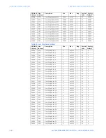
Page 183: ...s that correspond to the points provisioned in the User Map index 40524 0x020B to 40648 0x287 may be read from the Actual Values map area located at the addresses from 30524 0x020B to 30648 0x0287 MODBUS User Map Table 42 User Map Settings MODBUS Address Hex Address Description Min Max Step Format Code Factory Default 40524 20B User Map Address 1 30001 43763 1 F1 30305 40525 20C User Map Address 2...

Page 184: ...63 1 F1 30290 40567 236 User Map Address 44 30001 43763 1 F1 30291 40568 237 User Map Address 45 30001 43763 1 F1 30296 40569 238 User Map Address 46 30001 43763 1 F1 30297 40570 239 User Map Address 47 30001 43763 1 F1 30300 40571 23A User Map Address 48 30001 43763 1 F1 30301 40572 23B User Map Address 49 30001 43763 1 F1 30328 40573 23C User Map Address 50 30001 43763 1 F1 30329 40574 23D User ...

Page 185: ... 30001 40613 264 User Map Address 90 30001 43763 1 F1 30001 40614 265 User Map Address 91 30001 43763 1 F1 30001 40615 266 User Map Address 92 30001 43763 1 F1 30001 40616 267 User Map Address 93 30001 43763 1 F1 30001 40617 268 User Map Address 94 30001 43763 1 F1 30001 40618 269 User Map Address 95 30001 43763 1 F1 30001 40619 26A User Map Address 96 30001 43763 1 F1 30001 40620 26B User Map Add...

Page 186: ...ser Map Value 6 0 0xFFFF 1 F1 0 30530 211 User Map Value 7 0 0xFFFF 1 F1 0 30531 212 User Map Value 8 0 0xFFFF 1 F1 0 30532 213 User Map Value 9 0 0xFFFF 1 F1 0 30533 214 User Map Value 10 0 0xFFFF 1 F1 0 30534 215 User Map Value 11 0 0xFFFF 1 F1 0 30535 216 User Map Value 12 0 0xFFFF 1 F1 0 30536 217 User Map Value 13 0 0xFFFF 1 F1 0 30537 218 User Map Value 14 0 0xFFFF 1 F1 0 30538 219 User Map ...

Page 187: ...er Map Value 53 0 0xFFFF 1 F1 0 30577 240 User Map Value 54 0 0xFFFF 1 F1 0 30578 241 User Map Value 55 0 0xFFFF 1 F1 0 30579 242 User Map Value 56 0 0xFFFF 1 F1 0 30580 243 User Map Value 57 0 0xFFFF 1 F1 0 30581 244 User Map Value 58 0 0xFFFF 1 F1 0 30582 245 User Map Value 59 0 0xFFFF 1 F1 0 30583 246 User Map Value 60 0 0xFFFF 1 F1 0 30584 247 User Map Value 61 0 0xFFFF 1 F1 0 30585 248 User M...

Page 188: ...e 98 0 0xFFFF 1 F1 0 30622 26D User Map Value 99 0 0xFFFF 1 F1 0 30623 26E User Map Value 100 0 0xFFFF 1 F1 0 30624 26F User Map Value 101 0 0xFFFF 1 F1 0 30625 270 User Map Value 102 0 0xFFFF 1 F1 0 30626 271 User Map Value 103 0 0xFFFF 1 F1 0 30627 272 User Map Value 104 0 0xFFFF 1 F1 0 30628 273 User Map Value 105 0 0xFFFF 1 F1 0 30629 274 User Map Value 106 0 0xFFFF 1 F1 0 30630 275 User Map V...

Page 189: ...SFORMER PROTECTION SYSTEM COMMUNICATIONS GUIDE 1 185 30646 285 User Map Value 123 0 0xFFFF 1 F1 0 30647 286 User Map Value 124 0 0xFFFF 1 F1 0 30648 287 User Map Value 125 0 0xFFFF 1 F1 0 MODBUS Address Hex Address Description Min Max Step Format Code Factory Default ...

Page 190: ...1 186 345 TRANSFORMER PROTECTION SYSTEM COMMUNICATIONS GUIDE USING THE MODBUS USER MAP CHAPTER 1 COMMUNICATIONS GUIDE ...

Reviews: