B-18
C70 Capacitor Bank Protection and Control System
GE Multilin
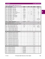
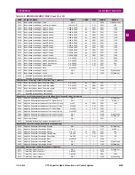
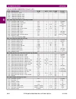
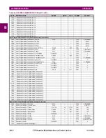
B.4 MEMORY MAPPING
APPENDIX B
B
3732
Time of day timer 3 state
0 to 1
---
1
F108
0 (Off)
3733
Time of day timer 4 state
0 to 1
---
1
F108
0 (Off)
3734
Time of day timer 5 state
0 to 1
---
1
F108
0 (Off)
Capacitor control actual values (read only)
3780
Capacitor control 1 discharge time
0 to 3600
s
1
F001
0
3781
Capacitor control 2 discharge time
0 to 3600
s
1
F001
0
3782
Capacitor control 3 discharge time
0 to 3600
s
1
F001
0
3783
Capacitor control 4 discharge time
0 to 3600
s
1
F001
0
Passwords (Read/Write Command)
4000
Command Password Setting
0 to 4294967295
---
1
F003
0
Passwords (Read/Write Setting)
4002
Setting Password Setting
0 to 4294967295
---
1
F003
0
Passwords (Read/Write)
4008
Command Password Entry
0 to 4294967295
---
1
F003
0
400A
Setting Password Entry
0 to 4294967295
---
1
F003
0
Passwords (read only actual values)
4010
Command password status
0 to 1
---
1
F102
0 (Disabled)
4011
Setting password status
0 to 1
---
1
F102
0 (Disabled)
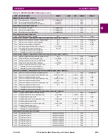
Passwords (read/write settings)
4012
Control password access timeout
5 to 480
minutes
1
F001
5
4013
Setting password access timeout
5 to 480
minutes
1
F001
30
4014
Invalid password attempts
2 to 5
---
1
F001
3
4015
Password lockout duration
5 to 60
minutes
1
F001
5
4016
Password access events
0 to 1
---
1
F102
0 (Disabled)
4017
Local setting authorization
1 to 65535
---
1
F300
1
4018
Remote setting authorization
0 to 65535
---
1
F300
1
4019
Access authorization timeout
5 to 480
minutes
1
F001
30
User Display Invoke (Read/Write Setting)
4040
Invoke and Scroll Through User Display Menu Operand
0 to 65535
---
1
F300
0
LED Test (Read/Write Setting)
4048
LED Test Function
0 to 1
---
1
F102
0 (Disabled)
4049
LED Test Control
0 to 65535
---
1
F300
0
Preferences (Read/Write Setting)
404F
Language
0 to 3
---
1
F531
0 (English)
4050
Flash Message Time
0.5 to 10
s
0.1
F001
10
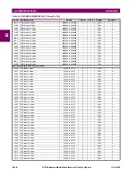
4051
Default Message Timeout
10 to 900
s
1
F001
300
4052
Default Message Intensity
0 to 3
---
1
F101
0 (25%)
4053
Screen Saver Feature
0 to 1
---
1
F102
0 (Disabled)
4054
Screen Saver Wait Time
1 to 65535
min
1
F001
30
4055
Current Cutoff Level
0.002 to 0.02
pu
0.001
F001
20
4056
Voltage Cutoff Level
0.1 to 1
V
0.1
F001
10
Communications (Read/Write Setting)
407E
COM1 minimum response time
0 to 1000
ms
10
F001
0
407F
COM2 minimum response time
0 to 1000
ms
10
F001
0
4080
Modbus Slave Address
1 to 254
---
1
F001
254
4083
RS485 Com1 Baud Rate
0 to 11
---
1
F112
8 (115200)
4084
RS485 Com1 Parity
0 to 2
---
1
F113
0 (None)
4085
RS485 Com2 Baud Rate
0 to 11
---
1
F112
8 (115200)
4086
RS485 Com2 Parity
0 to 2
---
1
F113
0 (None)
4087
IP Address
0 to 4294967295
---
1
F003
56554706
4089
IP Subnet Mask
0 to 4294967295
---
1
F003
4294966272
408B
Gateway IP Address
0 to 4294967295
---
1
F003
56554497
408D
Network Address NSAP
---
---
---
F074
0
409A
DNP Channel 1 Port
0 to 4
---
1
F177
0 (None)
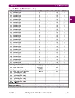
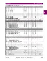
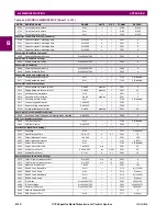
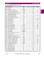
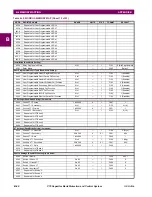
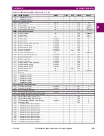
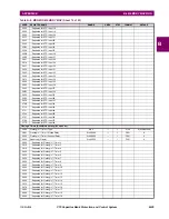
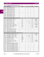
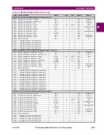
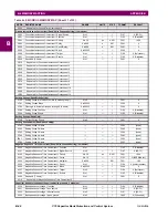
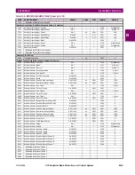
Table B–9: MODBUS MEMORY MAP (Sheet 11 of 53)
ADDR
REGISTER NAME
RANGE
UNITS
STEP
FORMAT
DEFAULT
Summary of Contents for UR Series C70
Page 2: ......
Page 10: ...x C70 Capacitor Bank Protection and Control System GE Multilin TABLE OF CONTENTS ...
Page 344: ...5 220 C70 Capacitor Bank Protection and Control System GE Multilin 5 10 TESTING 5 SETTINGS 5 ...
Page 586: ...D 10 C70 Capacitor Bank Protection and Control System GE Multilin D 1 OVERVIEW APPENDIXD D ...

