


Cinterion
®
LGA DevKit User Guide
10.2 Schematics
27
lga_devkit_ug_v02
2019-05-27
Preliminary
Page 25 of 28
GND
T27A1132-80SSG0PBNA01RTC
GN
D
GN
D
GN
D
0R
2x4_HEAD_SMD
0R_np
2x4_HEAD_SMD
2x4_HEAD_SMD
GND
47k
2x4_HEAD_SMD
2x4_HEAD_SMD
100nF
GND
100nF
GND
100nF
100nF
GND
GND
100nF
GND
GND
100nF
100nF
GND
GND
100nF
SSSS811101
GND
2x8_HEAD_SMD
2x6_HEAD_SMD
GND
470k
TLV6741_np
GND
0R
74LVCH2T45GT
74LVCH2T45GT
GND
GND
74LVCH2T45GT
74LVCH2T45GT
GND
GND
74LVCH2T45GT
74LVCH2T45GT
GND
74LVCH2T45GT
74LVCH2T45GT
GND
GND
BC847
BC847
47k
47k_np
0R
GN
D
GN
D
100nF_np
GN
D
100nF
4k7
0R
0R
0R
0R
0R
100R
100R
100R
100R
100R
74LVCH2T45GT
GND
74LVCH2T45GT
GND
74LVCH2T45GT
GND
74LVCH2T45GT
GND
100nF
100nF
100nF
100nF
GND
GN
D
GN
D
G
N
D
GN
D
100nF
100nF
100nF
GN
D
GN
D
GN
D
GN
D
2x6_HEAD_SMD
_np
GND
_np
_np
_n
p
_np
33pF
33pF
33pF
33pF
33pF
0R
GND
1uF
GND
B
C
847
10k
_np
_np
BC847
GND
47k
CDBQR70
ASC0.1
ASC0.2
ASC1
DAI
LGA DevKit S+M
U$1
GND
2
ADC1_IN
4
ADC2_IN
6
GND
8
TXD2_GPIO10
10
SD_WP(GPIO8)
12
SPIDI
14
SD_DET(GPIO7)
16
SD_CMD(GPIO6)
18
SD_CLK(GPIO5)
20
I2CCLK
22
VUSB_IN
24
USC5
26
ISENSE
28
USC6
30
CCCLK
32
VSIM
34
CCIO
36
CCRST
38
CCIN
40
CCGND
42
USC4
44
USC3
46
USC2
48
USC1
50
USC0
52
BATTEMP
54
SYNC
56
RXD1
58
RXD0
60
TXD1
62
TXD0
64
VDDLP
66
VCHARGE
68
CHARGEGATE
70
GND
72
GND
74
GND
76
GND
78
GND
80
BATT+
79
BATT+
77
BATT+
75
BATT+
73
BATT+
71
VEXT
69
RING0
67
DSR0
65
RTS0
63
DTR0
61
RTS1
59
CTS0
57
CTS1
55
DCD0
53
EMERG_RST
51
IGT
49
AGND
47
MICN1
45
MICP1
43
MICP2
41
MICN2
39
EPN1
37
EPP1
35
EPP2
33
EPN2
31
VMIC
29
VSENSE
27
USB_DN
25
USB_DP
23
I2CDAT
21
SD_0(GPIO1)
19
SD_1(GPIO2)
17
SD_2(GPIO3)
15
SD_3(GPIO4)
13
SPICS
11
RXD2_GPIO9
9
TP_ENV
7
PWR_IND
5
DAC_OUT
3
GND
1
R1
CON7
1
2
3
4
5
6
7
8
R2
CON11
1
2
3
4
5
6
7
8
CON13
1
2
3
4
5
6
7
8
R24
CON10
1
2
3
4
5
6
7
8
CON9
1
2
3
4
5
6
7
8
C24
C25
C26
C27
C28
C29
C32
C33
S2
A
B
S2
CON12
1
2
3
4
5
6
7
8
9
10
11
12
13
14
15
16
CON14
1
2
3
4
5
6
7
8
9
10
11
12
TP7
TP8
TP9
TP13
TP14
TP15
TP19
TP20
TP21
TP22
TP23
TP24
TP25
TP26
TP27
TP28
TP29
TP30
TP31
TP32
TP33
R51
IC8
3
1
4
5
2
TP34
TP35
TP36
TP100
TP38
TP39
TP40
TP41
TP37
TP42
TP43
TP44
TP45
TP46
TP47
TP48
R15
B1
7
A1
2
IC14
DIR
5
A2
3
B2
6
VCC-A
1
VCC-B
8
GND
4
B1
7
A1
2
IC15
DIR
5
A2
3
B2
6
VCC-A
1
VCC-B
8
GND
4
B1
7
A1
2
IC2
DIR
5
A2
3
B2
6
VCC-A
1
VCC-B
8
GND
4
B1
7
A1
2
IC16
DIR
5
A2
3
B2
6
VCC-A
1
VCC-B
8
GND
4
B1
7
A1
2
IC5
DIR
5
A2
3
B2
6
VCC-A
1
VCC-B
8
GND
4
B1
7
A1
2
IC17
DIR
5
A2
3
B2
6
VCC-A
1
VCC-B
8
GND
4
B1
7
A1
2
IC6
DIR
5
A2
3
B2
6
VCC-A
1
VCC-B
8
GND
4
B1
7
A1
2
IC18
DIR
5
A2
3
B2
6
VCC-A
1
VCC-B
8
GND
4
TP1
TP2
TP3
TP49
TP50
TP51
T2A
T2B
R49
R50
R59
C58
C60
R61
R64
R65
R66
R67
R68
R69
R70
R71
R72
R73
B1
7
A1
2
IC3
DIR
5
A2
3
B2
6
VCC-A
1
VCC-B
8
GND
4
B1
7
A1
2
IC19
DIR
5
A2
3
B2
6
VCC-A
1
VCC-B
8
GND
4
B1
7
A1
2
IC21
DIR
5
A2
3
B2
6
VCC-A
1
VCC-B
8
GND
4
B1
7
A1
2
IC22
DIR
5
A2
3
B2
6
VCC-A
1
VCC-B
8
GND
4
C59
C61
C62
C63
C64
C65
C66
JP6
1
2
3
4
5
6
7
8
9
10
11
12
JP7
1
2
3
4
SCL
1
VSS
2
SDA
3
VCC
4
NC
5
TP52
TP53
TP54
TP55
C67
C68
C69
C70
C71
R82
C72
T3
A
R83
TP59
TP60
T3B
R89
TP11
TP12
TP16
TP17
TP18
TP73
TP74
TP82
TP83
D4
RTS0_X100/[2]
RTS0_X100/[2]
CTS0_X100/[2]
CTS0_X100/[2]
DTR0_X100/[2]
DTR0_X100/[2]
DSR0_X100/[2]
DSR0_X100/[2]
DCD0_X100/[2]
DCD0_X100/[2]
TXD0_X100/[2]
TXD0_X100/[2]
RXD0_X100/[2]
RXD0_X100/[2]
RING0_X100/[2]
RING0_X100/[2]
CTS1_X100
CTS1_X100
EMERG_RST_X100/[1]
EMERG_RST_X100/[1]
AGND_X100
AGND_X100
MICN1_X100
MICN1_X100
MICP1_X100
MICP1_X100
MICP2_X100
MICN2_X100
EPN1_X100
EPN1_X100
EPP1_X100
EPP1_X100
EPP2_X100
EPN2_X100
VMIC_X100
VMIC_X100
I2CDAT_X100
I2CDAT_X100
SD_0_X100
SD_1_X100
SD_2_X100
SD_3_X100
SD_3_X100
SPICS_X100
RXD2_GPIO9_X100
TP_ENV_X100
DAC_OUT_X100
ADC1_IN_X100
ADC1_IN_X100
ADC2_IN_X100
TXD2_GPIO10_X100
SD_WP(GPIO8)_X100
SD_WP(GPIO8)_X100
SPIDI_X100
SD_DET(GPIO7)_X100
SD_DET(GPIO7)_X100
SD_CMD(GPIO6)_X100
SD_CMD(GPIO6)_X100
SD_CLK(GPIO5)_X100/[2]
SD_CLK(GPIO5)_X100/[2]
SD_CLK(GPIO5)_X100/[2]
I2CCLK_X100
I2CCLK_X100
USC5_X100
USC6_X100
CCIN_X100/[1]
USC4_X100
USC3_X100
USC3_X100
USC2_X100
USC2_X100
USC1_X100
USC1_X100
USC0_X100
USC0_X100
SYNC_X100
SYNC_X100
RXD1_X100
RXD1_X100
TXD1_X100
TXD1_X100
RTS1_X100
RTS1_X100
AGND/[1]
AGND/[1]
VMIC/[1]
VMIC/[1]
MICN1/[1]
MICN1/[1]
EPP1/[1]
EPP1/[1]
EPN1/[1]
EPN1/[1]
MICP1/[1]
MICP1/[1]
I2CCLK/[2]
I2CDAT/[2]
ADC1/[1]
FSDAI/[1]
RXDAI/[1]
TXDAI/[1]
GPIO8/[1]
GPIO7/[1]
GPIO6/[1]
GPIO5/[1]
GPIO4/[1]
RXD1/[1]
TXD1/[1]
CTS1/[1]
RTS1/[1]
RXD0/[1]
TXD0/[1]
CTS0/[1]
RTS0/[1]
DCD0/[1]
DTR0/[1]
DSR0/[1]
RING0/[1]
EMG_RST/[1]
CCIN/[1]
SCLKDAI/[1]
ON/[1]
ON_MODULE/[1]
X100.BATT+/[2]
RXD0@LS
RXD0@LS
TXD0@LS
TXD0@LS
CTS0@LS
CTS0@LS
RTS0@LS
RTS0@LS
DCD0@LS
DCD0@LS
DTR0@LS
DTR0@LS
RING0@LS
RING0@LS
DSR0@LS
DSR0@LS
CTS1@LS
CTS1@LS
RTS1@LS
RTS1@LS
RXD1@LS
RXD1@LS
TXD1@LS
TXD1@LS
FTDI_RESET/[2]
FTDI_RESET/[2]
V480/[2]
V480/[2]
VEXT_BUFF/[2]
VEXT_BUFF/[2]
VEXT_BUFF/[2]
VEXT_BUFF/[2]
VEXT_BUFF/[2]
VEXT_BUFF/[2]
VEXT_BUFF/[2]
VEXT_BUFF/[2]
VEXT_BUFF/[2]
VEXT_BUFF/[2]
VEXT_BUFF/[2]
VEXT_BUFF/[2]
USC3@LS
USC3@LS
USC2@LS
USC2@LS
USC1@LS
USC1@LS
USC0@LS
USC0@LS
VEXT_MODULE/[1]
VEXT_JUMPER/[2]
VREF/[2]
VREF/[2]
VREF/[2]
VREF/[2]
VREF/[2]
VREF/[2]
VREF/[2]
VREF/[2]
VREF/[2]
VREF/[2]
PWR_IND
PWR_IND
VCORE/[1]
BATT+/[2]
BATT+/[2]
GND_DETECT_DSB/[2]
CCCLK2/[1]
CCVCC2/[1]
CCIO2/[1]
CCRST2/[1]
CCIN2/[1]
1LS_OUT_B1
1LS_OUT_B1
1LS_OUT_B2
1LS_OUT_B2
2LS_IN_B1
2LS_IN_B1
2LS_IN_B2
2LS_IN_B2
2LS_OUT_A1
2LS_OUT_A1
2LS_OUT_A2
2LS_OUT_A2
1LS_IN_A1
1LS_IN_A1
1LS_IN_A2
1LS_IN_A2
I2C_DAT_LS/[2]
I2C_CLK_LS/[2]
+3V/[1]
LDO_OUT/[2]
MOD_ON_DET/[1]
IGT_X100/[1]
Änderung
Datum
Nam.
Datum
Name
Bear.
Gepr.
Vers.:
Blatt:
Ers. f.:
Ers. d.:
BG:
A
B
C
D
E
F
G
H
H
G
F
E
D
C
B
A
5
2
1
1
2
3
4
5
4
3
GND
VCC
GND
H
L
H
L
H
L
H
L
H
L
H
L
H
L
H
L
H
L
H
L
H
L
H
L
@LS = LEVELSHIFTER
If DevKit is used as
DSB Adapter this pin is low
Control
ASC0.1
ASC0.2
ASC1
DAI
AUDIO2
GPIO
= ENABLE RS232/LEVELSHIFTER*
= ENABLE FTDI ONBOARD
*The equivalent switch on DSB Mini
must be set to RS232
SCLK
FS
RXDDAI
TXDDAI
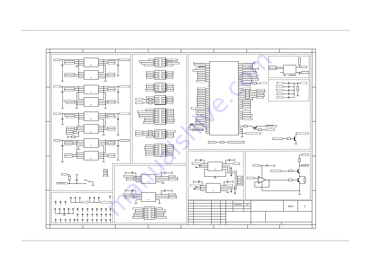
PINHEADER
80 PIN INTERFACE
PATCHFIELD
LEVEL SHIFTER
POWER INDICATION CICUIT
FREE LEVELSHIFTER PATCHFIELD
FREE LEVELSHIFTER PINHEADER
EEPROM
>A=
>B=


