

User Manual
GD32350R-EVAL
10 /33
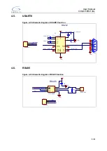
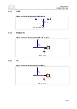
4.7.
ADC/DAC
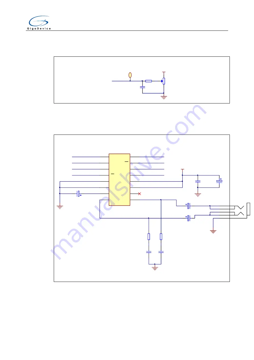
Figure 4-7 Schematic diagram of ADC/DAC function
+3V3
GND
ADC
C1
50V/0.1uF
R1
1K
Ω
PC1
VR1
10K
1
TP1
TP ADin
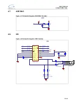
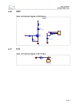
4.8.
I2S
Figure 4-8 Schematic diagram of I2S function
LRCK
1
DATA
2
BCK
3
PD
4
AGND
5
HGND
6
Vcom
7
HoutR
8
SCKI
16
HoutL
9
AIN
10
Vhp
11
VCC
12
MD
13
MC
14
MS
15
U2
PCM1770 PM
NRST
GND
+3V3
E2
16V/10uF,AVX
5
4
3
2
1
J1
HeadPhone
E3
10V/220uF,AVX
E4
10V/220uF,AVX
R7
16R
R8
16R
C5
50V/0.22uF
C6
50V/0.22uF
GND
C4
50V/0.1uF
E1
16V/10uF,AVX
GND
GND
PA4
PA7
PA5
PA6
PA15
I2S
I2S_WS
I2S_DIN
I2S_CK
I2S_MCK
MSEL
MCLK
MDIN
I2S_MCLK
I2S_MDIN


