Minimal Design for GR551x SoC
When designing the layout, make sure the main chip is as close to the antenna interface as possible, and no other
components are under the RF routing if possible (the layout and routing of RF components are of higher priority).
3.2.3 Power Supply
Power supply is essential to ensure proper operation of an SoC, and therefore special attention should be paid on the
layout and routing of the key power systems, which are DC-DC switching regulator and RF input power supply. To avoid
system-level issues (such as poor performance in ESD protection and radiation off limits) caused by improper power
design, abide by the design hints described in the two following sections.
3.2.3.1 DC-DC Switching Regulator
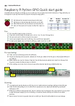
Take GR5515RGBD for example. The chip includes a DC-DC switching regulator. To design the PCB layout involving a
DC-DC switching regulator,
1.
Components (L3: 9.1 nH inductor, L4: 2.2 µH inductor, and C15: 2.2 µF capacitor) connected to DC-DC switching
regulator should be placed as close to VSW and VREG of the chip as possible. A distance within 3 mm is
recommended.
2.
The net of VSW radiates stronger interference before VSW signals passing through the inductors, and thus should
be placed at a minimum distance of 0.2 mm from other power nets and signals, especially V1P0 and DIGCORE.
3.
Placing L4 perpendicular to L3 is recommended, to avoid inductive coupling. C15 should be placed behind L4, and
VREG network is connected to the power supply after capacitor filtering.
4.
GND pin of C15 should be placed as close to VSS_BUCK of the chip as possible. Vias of C15 GND pin should be
placed as close to the GND pin as possible. It is recommended to connect the C15 GND pin to VSS_BUCK by using
GND Polygon Plane, so that the return path of the power can be kept minimal.
Figure 3-7 Reference layout and routing for DC-DC switching regulator
Copyright © 2021 Shenzhen Goodix Technology Co., Ltd.
33


