Minimal Design for GR551x SoC
Note
:
The green line in the right figure of
indicates the power output path.
3.2.3.2 RF Input Power Supply
Make sure the following instructions are met when designing RF input power supply in PCB layout, to ensure optimal
performance and to avoid excessively high radiation.
1.
Decoupling capacitors (highlighted in yellow rectangles in
) connected to VDD_RF, VDD_VCO, and
VDD_AMS should be as close to the corresponding pin as possible (around 1 mm is recommended, and shall
not exceed 3 mm). Place the capacitors on the same layer with the pins if possible, and make sure the wiring
path goes through the capacitors first and then connected to the chip power pins. In case the capacitors are not
placed on the same layer with the pins, the vias should be located close to the decoupling capacitors.
2.
The power trace should be as short as possible, and at least 0.2 mm wide. A minimum distance at 0.2 mm from
other signals should be guaranteed.
D<3mm
D<3mm
D<3mm
D<3mm
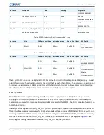
Figure 3-8 Reference layout and routing for RF input power supply
C1 (10 μF capacitor) is placed close to the VBATL pin; C4, C7, and C8 (0.1 μF capacitors) are placed close to the
VDD_VCO, VDDIO1, and VIO_LDO_OUT respectively, and C2, C3, and C6 (15 pF capacitors) close to VDD_AMS,
VBATT_RF, and VDD_RF respectively. C5 (1 μF capacitor) is placed close to pin VDD_DIGCORE_1V, as shown in
Copyright © 2021 Shenzhen Goodix Technology Co., Ltd.
34


