Minimal Design for GR551x SoC
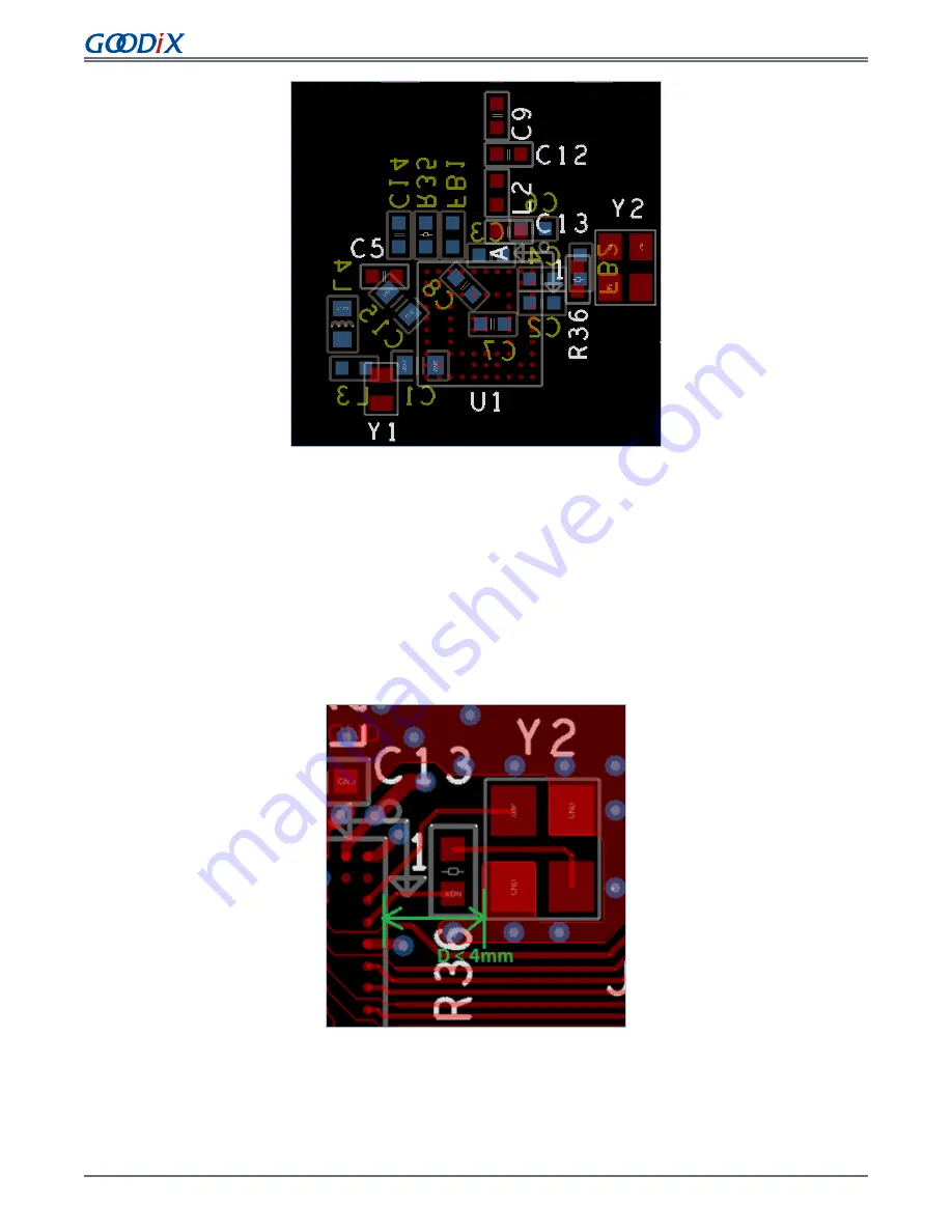
Figure 3-9 Power supply of GR5515RGBD PCB (reference)
3.2.4 Clock
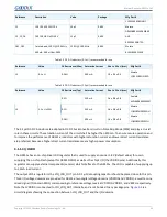
Place the crystal as close as possible to the IC (recommended distance: ≤4 mm). This will minimize any additional
capacitive load on the input pins and reduce the chance of crosstalk and interference with other signals on the board.
Make sure there is no other trace route next to/under the crystal or the crystal routes.
It is recommended to shield the routes of the 32 MHz crystal. If the ground below the crystal is clean and no crosstalk
or interference is involved, provide openings on the pad underneath the crystal (as shown in
), which helps
to reduce parasitic capacitance.
Figure 3-10 Clock PCB Ref of GR5515RGBD (reference)
Copyright © 2021 Shenzhen Goodix Technology Co., Ltd.
35


