Minimal Design for GR551x SoC
3.2.7.1 System-level ESD Design
System efficient electrostatic discharge (ESD) design is crucial for any circuits, and requires users to follow the design
guidelines (including schematic diagrams, PCB layout, and product structural designs) provided in the sections below.
3.2.7.1.1 ESD Schematic Design
1.
GR551x series is powered by an independent external LDO regulator (see “
” for
details).
2.
To suppress static voltages, connect a ferrite bead to each of the two charging ports (CHAR+ and CHAR-) in series,
and apply a proper transient voltage suppressor (TVS) diode at each ferrite bead to found the basis of the ESD
protection scheme, as shown in the figure below.
ESD=5V TVS
FB1=600
Ω
BLM15PX601SN1
FB2=600
Ω
BLM15PX601SN1
CHAR+
CHAR-
Charge IC
GND
GR551x
LDO
Lithium baery
VBATL
POWER IN
BAT+
Figure 3-13 ESD protection scheme at charging ports
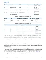
Recommended models of TVS diodes and ferrite beads, as well as model selection requirements, are listed in the
tables below.
Table 3-11 Model selection for TVS diodes
Parameters
Description
Min.
Typ.
Max.
V
RwM
(V)
Reverse working maximum voltage
-
5 V
-
V
BR
(V)
Breakdown voltage
-
7 V
-
V
clamp
(V)
Clamp voltage
-
6 V
-
V
ESD
(kV)
ESD prevention performance
•
Contact discharge: ±10 kV
•
Air discharge: ±12 kV
-
-
Table 3-12 Model selection for ferrite beads
Parameters
Description
Min.
Typ.
Max.
Impedance@100 MHz (Ω)
Impedance @ 100 MHz
-
600 Ω
-
I
R
(mA)
Rated operating current
-
900 mA
-
R
DC
Max. (mΩ)
Maximum DC resistance
-
230 mΩ
-
Copyright © 2021 Shenzhen Goodix Technology Co., Ltd.
38


