Minimal Design for GR551x SoC
Reference
Description
Value
Package
Mfg Part #
CL05A105KO5NNNC
C1
CAP CER X5R 20% 10 V
10 µF
0603
Murata
GRM188R61A106ME69
C2, C3, C6
CAP CER NPO ±5% 50 V
15 pF
0603
AVX
04025A150JAT2A
FB1, FB2
Ferrite Bead, 120 Ω @ 100 MHz,
400 mA, 500 mOhm, 0603
120 Ω @ 100 MHz
0603
Murata
BLM18AG121SN1
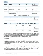
Table 3-2 DC-DC inductors (9.1 nH) recommended for use
Reference
Value
DC Resistance (Max) Saturation Current
Size L x W x H (mm) Mfg Part #
L3
9.1 nH
0.26 Ω
500 mA
1.0 x 0.5 x 0.5
Murata
LQG15HS9N1J02D
Table 3-3 DC-DC inductors (2.2 µH) recommended for use
Reference
Value
DC Resistance (Typ) Saturation Current
Size L x W x H (mm) Mfg Part #
0.3 Ω
250 mA
1.6 x 0.8 x 0.8
Sunlord
MPH160809S2R2MT
0.2 Ω
250 mA
1.6 x 0.8 x 0.8
Murata
LQM18PN2R2MGH
L4
2.2 µH ± 20%
0.38 Ω
300 mA
1.6 x 0.8 x 0.8
Murata
LQM18PN2R2MFH
The 2.2 µH DC-DC inductors are adopted in DC-DC buck converter circuits in Pulse Skip Mode (PSM) and play a crucial
role in these circuits. The saturation current of the circuit shall be higher than 250 mA. To ensure secure operation and
to improve the performance of GR551x, inductors with higher saturation current and lower direct current resistance
are preferred, because a higher direct current resistance means higher power consumption.
3.1.1.3 I/O LDO
The GR551x has an on-chip linear LDO regulator that is used to supply a nominal 1.8 V (default value) for use in
supplying the on-chip Flash (except for GR5515I0ND) as well as the chip’s I/O (the VDDIO0 pins). Additionally, this
regulator can supply external components (sensors) which interface to the GR551x. The LDO is capable of supplying up
to 30 mA load current.
The output of this regulator is the VIO_LDO_OUT pin. A 0.1 μF decoupling capacitor should be placed close to this pin.
Three I/O voltage domains are provided for GR551x: two digital voltage domains (VDDIO0 and VDDIO1), as well as one
mixed signal I/O domain MSIO, corresponding to reference voltage levels at VDDIO0, VDDIO1, and VBATL respectively.
Note that VDDIO0 is connected to VIO_LDO_OUT internally, and is not bonded to any package pins.
is a
circuit diagram showing the connection between VIO_LDO_OUT and the I/O domains.
Copyright © 2021 Shenzhen Goodix Technology Co., Ltd.
25


