Minimal Design for GR551x SoC
VBATL
VBATL
VIO_LDO_OUT
Default 1.8V,30mA
VDDIO1
IO_LDO
Stacked Flash (Except
for GR5515I0ND)
VDDIO0
(GPIO16-31,
AON_GPIO0-7)
VDDIO1
(GPIO0-15)
MSIO0-7
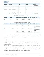
Figure 3-3 Connection between VIO_LDO_OUT and I/O domains
Note
:
The leakage current of I/O LDO is approximately 0.7 µA.
VIO_LDO_OUT is connected to the power of Flash on chip. The operating voltage of Flash is 1.8 V (except for the
Flash of GR5515I0ND), and therefore the default voltage of VIO_LDO_OUT is 1.8 V. When VDDIO1 is connected to
VIO_LDO_OUT on an external circuit, the I/O voltage domains of the chip is 1.8 V (except for MSIOs). If you need
to change the I/O voltage domain corresponding to VDDIO1, use an external power supply (voltage range: 1.8 V –
3.3 V) for VDDIO1. In this process, the levels of the GPIOs corresponding to VDDIO1 vary, depending on the external
input voltage. When the external power supply is connected to VDDIO1, make sure the input voltage at VDDIO1 is not
higher than that of the power (VBATL).
The Flash of GR5515I0ND supports operations in high-voltage scenarios (when VDDIO0 = 3.3 V/VBATL). To use the SoC
in high voltage scenarios,
•
I/O LDO is set to off mode automatically based on eFuse configurations after system startup.
•
Use VIO_LDO_OUT as input for the VDDIO0 domain, and connect VIO_LDO_OUT to the external power supply of
3.3 V or VBATL.
Copyright © 2021 Shenzhen Goodix Technology Co., Ltd.
26


