Minimal Design for GR551x SoC
The following figure is the recommended RF matching circuit in the GR5551x SoC minimal system.
Figure 3-5 RF scheme
In the circuit, the left PI matching network (composed of the inductor L1 plus capacitors C10 and C11) matches
the antenna; C9 is a DC blocking capacitor; the right PI type matching network (composed of the inductor L2 plus
capacitors C12 and C13) matches the internal PA of GR551x. The network connects to the TRX pin of the chip.
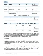
Recommended configurations of capacitors C12, C13, C9, and the inductor L2 are displayed in
Table 3-8 Recommended devices for the RF section
Reference Description
Value
Package Size Mfg Part #
C9
CAP CER NPO 5% 50 V
18 pF
0402
Murata GRM1555C1H180JA01D
C12
CAP CER NPO 0.8 pF+/–0.05 pF 50 V
0.8 pF
0402
Murata GRM1555C1HR80WA01D
C13
CAP CER NPO 2.0 pF+/–0.1 pF 50 V
2.0 pF
0402
Murata GRM1555C1H2R0BA01D
L2
Inductor, Wirewound, 2.4 nH, 0.2 nH, 50 mOhm,
Q = 20 @ 250 MHz
2.4 nH
0402
Murata
LQW15AN2N4B00
3.1.4 I/O Pins
The GR551x has software-configurable I/O pin assignment where different peripherals can be multiplexed out on
different chip pins. When configured to GPIOs, they can be set as input, output, with configurable pull-up or pull-down
resistors. I/O pins retain their last state when system enters the sleep or deep sleep mode. Only AON_GPIOs can be
used to wake up the system from sleep/deep sleep mode.
Note
:
•
For more details of pin mux, refer to
GR551x Datasheet
.
•
Note that MSIO pins do not support hardware interrupt when allocating I/O functions during designing PCB
applications.
•
Two PWM modules(PWM0 and PWM1) are provided, with each containing three separate output channels:
PWMA, PWMB, and PWMC. Frequencies of the three PWM channels in one group are the same, and individual
frequency control is not supported. Phase and duty cycle of each channel can be configured via registers.
3.1.5 SWD Interfaces
GR551x connects to J-Link for modulation by using Serial Wire Debug (SWD) interfaces.
Copyright © 2021 Shenzhen Goodix Technology Co., Ltd.
30


