Reference Design
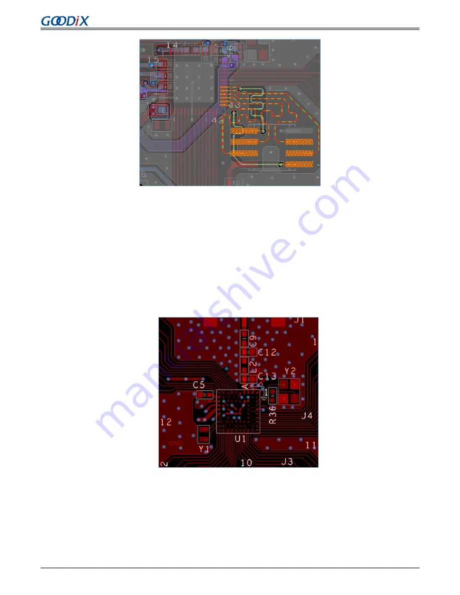
Figure 4-13 Reference design for GR5515I0ND PCB layout
4.2.4 Four-layer PCBs in BGA68 Package(NRND)
In this reference design, all GPIO signals are used as output. The 1.6 mm PCB is composed of four layers with PTHs.
The RF route is 22 mil wide, which is the same with the component pad. As specified in “
”, L2 is used
as the reference plane for the 50 Ω RF transmission line.
Details for the PCB layout reference design are provided below.
1.
Top layer
This layer is used for component layout and routing for key signals such as RF.
Figure 4-14 Top layer design for 4-layer PCB (BGA68)
2.
L2
This is the reference ground plane for the ground return path of the 50 Ω RF transmission line. Two openings are
provided underneath the signal output pads of the 32 MHz crystal on L2, to reduce the parasitic load capacitance
of the crystal.
Copyright © 2021 Shenzhen Goodix Technology Co., Ltd.
53


