All Rights reserved, No Spreading without GOSUNCN Permission
35
Hardware Development Guide
ME3616
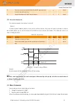
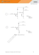
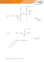
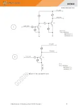
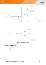
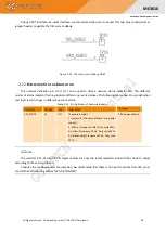
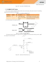
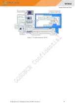
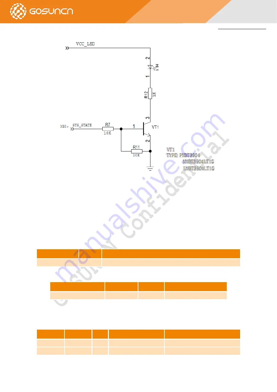
Figure 2-26
Connections of the
SYS_STATE
pin
2.13.
ADC
I
NTERFACE
The module provides one ADC to digitize the analog signal to 10-bit digital data such as battery voltage,
temperature and so on. Using AT command “AT+ZADC?” can read the voltage value on ADC pin.
The read value is
expressed in mV. For more details of these AT commands,
please
refer to document
[AT Command Reference Guide of Module
Product ME3616]
.
In order to improve the accuracy of ADC, the trace of ADC should be surrounded by ground.
Table 2-15 Pin Definition of the ADC
Pin Name
Pin NO.
Description
ADC1
38
General purpose analog to digital converter.
The following table describes the characteristic of the ADC function
Table 2-16 Characteristic of the ADC
Item
Min
Max
Unit
ADC voltage range
0
1.4
V
2.14.
GPIO
I
NTERFACE
ME3616
Module provides 2 GPIO pins.
Table 2-17 Pin Definition of GPIO
Pin Name
Pin NO.
I/O
Description
Comment
GPIO1
34
IO
General input/output
1.8V power domain,
GPIO2
35
IO
General input/output
1.8V power domain

