3 Functional Description
3.2 USB 2.0 SoftPHY External Circuit Connection
IPUG781-1.5.1E
8(12)
2. You can see the followings for the IO port attribute constraints of GW1N series of
FPGA.
usb_dxp_io: IO_TYPE= LVCMOS33D PULL_MODE= NONE DRIVE=8;
usb_term_dn_o: IO_TYPE=LVCMOS33 PULL_MODE= NONE DRIVE=16;
usb_term_dp_o: IO_TYPE=LVCMOS33 PULL_MODE= NONE DRIVE=16;
usb_pullup_en_o: IO_TYPE=LVCMOS33 PULL_MODE= NONE DRIVE=8;
usb_rxdn_i: IO_TYPE=LVDS25 PULL_MODE=NONE;
usb_rxdp_i: IO_TYPE=LVDS25 PULL_MODE=NONE.
3. All signals related to the USB interface on the FPGA are recommended to be placed in
one Bank, using adjacent assignment, and powering the I/O Bank at 3.3V
4.
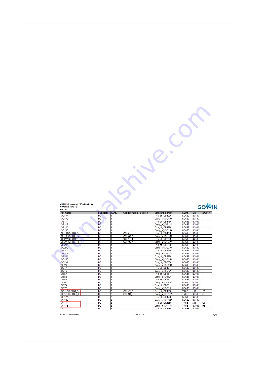
It is required that the adjacent differential pair pins in the same Bank where the
usb_dxp_io differential pair is located exist and are not used. Taking GW1NSR-4 as
shows the GW1NSR-4 Pinout. If the usb_dxp_io differential
pair is located at G5, H5 (i.e. IOR11A/IOR11B) in the diagram, it will cause the
project to report an error when implementing synthesis and placement with Gowin
Software, as the adjacent differential pair pins IOR10A/IOR10B do not exist. If
usb_dxp_io differential pair is located at G6/H6 (i.e. IOR13A/IOR13B), the project
will synthesize and place successfully with Gowin Software, as the adjacent
differential pair pins IOR12A/IOR12B exists.
Figure 3-3 GW1NSR-4 Pinout


