COMPONENT MAINTENANCE MANUAL
IN 1502H RADAR INDICATOR
TM109102
1-34
May/01
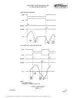
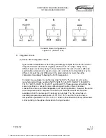
Simplified Schematic, LVPS On/Off Circuit
Figure 1-6
(2) Voltage-Controlled Oscillator
Integrated circuit U5003 is a TTL voltage controlled oscillator (VCO) that provides
complementary squarewave outputs. External resistance R5033 and capacitance
C5010 have been selected to provide an operating frequency range of 5 to 38 KHz.
Frequency is controlled by the voltage to the voltage sensitive input at pin 13.
Frequency increases as voltage increases, with zero volts producing the minimum
frequency and +5 volts producing maximum frequency. This voltage is controlled by
the outputs from regulator U5002C and current limiter U5002B. These circuits are
explained later.
The complementary TTL squarewave outputs are present at pins 6 and 8. Zener
diode CR5009 regulates the +12 volts down to 5 volts to obtain supply voltage for
U5003.
(3) Driver Circuit
The driver circuit consists of power transistors Q5001 through Q5006, proportional
drive transformers T5001 and T5002 and associated components. The LVPS is a
resonant mode power supply. It is triggered by the outputs from VCO U5003, but once
triggered, its output is determined by resonance of the series LC circuit formed
primarily by transformer T5003 and capacitor C5001.
Transistors Q5005 and Q5006 are switched on alternately by the positive going edges
of the complementary squarewave outputs of VCO U5003. These outputs are
differentiated to provide narrow positive spikes alternately to the bases of Q5005 and
Q5006 to switch on first one transistor and then the other. The positive edge of the
squarewave at pin 6 of U5003 rapidly charges C5003, via R5014, to produce the
positive spike at the base of Q5005. The positive edge of the squarewave at pin 8 of
U5003 triggers Q5006 in an identical manner.
The document reference is online, please check the correspondence between the online documentation and the printed version.


