background image

Vertiga UMS 5100

Allgemeiner Teil / General Section

GRUNDIG Service

1 - 9

ENGLISH

5

ENGLISH

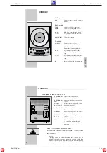
OVERVIEW

__________________________________________________________________________________

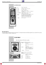
AUX operation

AUX

Selects the input source »

AUX

« (external

device).

Radio mode

TUNER

Selects the »

TUNER

« input source.

BAND

Selects the frequency band »

FM

« or

»

MW

«.

ıı

s6

Hold down to start the station search.

5a

ľľ

Press briefly to change the frequency in
small steps.

NEXT PRESET

Selects preset stations.

CD mode

CD/

ı

II

Selects the »

CD

« input source.

Starts and interrupts CD playback.

Ends CD playback.
Deletes the track memory for the CD.

ıı

s6

Press briefly to select the next track.
Hold down to look for a particular pas-
sage.

5a

ľľ

Press briefly to select the previous track.
Hold down to look for a particular pas-
sage.

ə

Opens and closes the CD compartment.

6

OVERVIEW

__________________________________________________________________________________

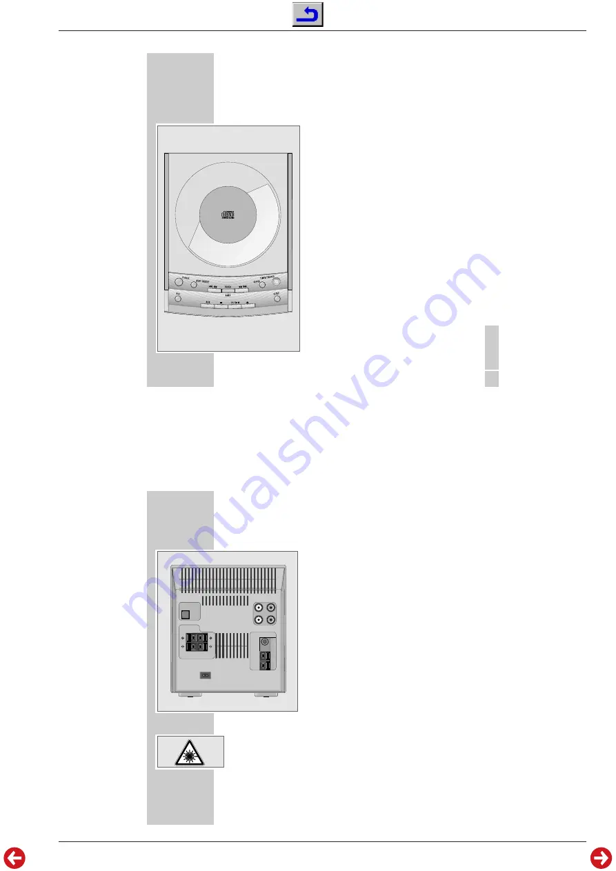
The back of the stereo system

ANTENNA FM

Socket for the rooftop antenna 

EXT

or the wire antenna supplied.

ANTENNA AM

Antenna terminals for the wire antenna

EXT

supplied.

OPTICAL

Digital output for copying a CD onto a

DIGITAL OUT 

digital recording device.

LINE IN (AUX)

Audio signal input for an external devi-
ce.

LINE OUT

Audio signal output for an external devi-
ce.

SPEAKERS

Connections for the loudspeakers 

R L  +    R L–

supplied.

R

= right channel, 

L

= left channel.

~ AC IN

Socket for power cord.
The only way to separate the stereo
system from the mains is to pull out the
mains plug.

General instructions for laser devices

The laser installed in the device conforms to LASER CLASS 1 and is designed to
ensure that the maximum permissible emission value cannot be exceeded under
any circumstances.

Caution:

If operating devices or methods other than those specified here are
employed, it may lead to dangerous exposure to emissions. Invisible laser
radiation is emitted if the CD compartment is opened or the safety locking
mechanism is shorted. Do not expose yourself to this radiation.

OPTICAL
DIGITAL OUT

SPEAKERS

IMPEDANCE MIN 4

LINE IN (AUX)

LINE OUT

R

R

L

L

ANTENNA

COA-
XIAL
75

AM

LOOP

AM

EXT

FM

EXT

˜ AC IN

R

L
Summary of Contents for GLL0252

Page 1: ...180 52318 42 0180 52318 43 0180 52318 44 0180 52318 45 0180 52318 51 0180 52318 99 Mo Fr 8 00 18 00 Uhr Telefon 0180 52318 40 0180 52318 50 Fax Technik Ersatzteil Verkauf Mo Fr 8 00 19 00 Uhr Kundendi...

Page 2: ...and Spare Parts List 4 1 4 4 Inhaltsverzeichnis Seite Allgemeiner Teil 1 2 1 8 Messger te Messmittel 1 2 Technische Daten 1 3 Servicehinweise 1 3 Ausbauhinweise 1 4 Bedienhinweise 1 6 Abgleichvorschr...

Page 3: ...ESET button on the bottom of the set using a small screw driver or a paper clip This will delete all stored settings Technische Daten Verst rkerteil Ausgangsleistung Sinusleistung 2 x 8W Musikleistung...

Page 4: ...rve the way they are routed On completion of the repairs the leads must be laid out as originally fitted at the factory 1 Cabinet Undo 7 screws A Fig 1 and 2 screws C Fig 2 Pull off the back panel B U...

Page 5: ...urch statische Aufladung zerst rt werden 4 Schrauben S Fig 9 herausdrehen und die CD Leiterplatte herausnehmen BeiBedarfdieMotoranschl sseT Fig 9 abl ten 3 Removing Tuner Board Remove bottom plate par...

Page 6: ...Bedienelemente an der Oberseite TIMER SNOOZE Zum Einstellen des Einschalt Timers unterbricht das Wecken f r ca 5 Min CLOCK Zum Einstellen der Uhrzeit SLEEP Zum Einstellen des Sleep Timers X BASS Zum A...

Page 7: ...as CD Fach ge ffnet oder die Sicherheitsverriegelung berbr ckt wird Nicht dem Strahl aussetzen OPTICAL DIGITAL OUT SPEAKERS IMPEDANCE MIN 4 LINE IN AUX LINE OUT R R L L ANTENNA COA XIAL 75 AM LOOP AM...

Page 8: ...r cken w hlt einen Titel an l ngeres Dr cken sucht eine bestimmten Passage Im CD Betrieb beendet die Wiedergabe der CD VOLUME ndert die Lautst rke TIMER SNOOZE CLOCK 1 2 3 4 5 6 7 8 9 10 SLEEP 0 REPEA...

Page 9: ...cket for the rooftop antenna EXT or the wire antenna supplied ANTENNA AM Antenna terminals for the wire antenna EXT supplied OPTICAL Digital output for copying a CD onto a DIGITAL OUT digital recordin...

Page 10: ...e selects the RDS time RDS In tuner mode selects the RDS mode DISPLAY In tuner mode calls up various information on the display TIMER SNOOZE CLOCK 1 2 3 4 5 6 7 8 9 10 SLEEP 0 REPEAT STEREO MONO RANDO...

Page 11: ...Eingang Ue 60dB V Oszilloskop ber 100nF an Messpunkt A AM 522kHz Digital Voltmeter an Messpunkt B AM Mess Sender ber Loop Antennen ankoppeln Ue 50dB V fmod 1kHz Oszilloskop an Lautsprecher Ausgang FM...

Page 12: ...o AM Aerial Input Ue 60dB V Oscilloscope via 100nF to Testpoint A AM 522kHz Digital Voltmeter to Testpoint B AM Couple Signal Generator via Loop Antennas Ue 50dB V fmod 1kHz Oscilloscope to Loudspreak...

Page 13: ...en Circuit Diagrams and Layout of the PCBs Vertiga UMS 5100 Schaltpl ne und Platinenabbildungen Circuit Diagrams and Layout of the PCBs 3 2 3 1 Schaltpl ne und Platinenabbildungen Circuit Diagrams and...

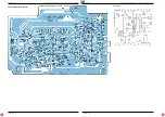
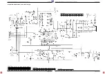
Page 14: ...Tuner Platte Tuner Board IC2 LA1832 PIN 1 2 3 4 5 6 7 8 9 10 11 12 FM 2 11 4 94 2 11 2 1 0 02 4 99 4 93 2 81 4 95 0 3 79 3 79 AM 2 11 4 95 2 1 2 09 0 4 95 0 3 71 4 96 0 02 1 6 0 79 PIN 13 14 15 16 17...

Page 15: ...Vertiga UMS 5100 Schaltpl ne und Platinenabbildungen Circuit Diagrams and Layout of the PCBs Vertiga UMS 5100 Schaltpl ne und Platinenabbildungen Circuit Diagrams and Layout of the PCBs 3 6 3 5 Tuner...

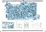
Page 16: ...e 3 16 IC201 LA4725A PIN 1 2 3 4 5 6 7 8 9 10 11 12 1 49 5 5 0 3 2 2 32 1 47 2 1 5 18 5 16 0 5 15 0 PIN 13 14 5 05 11 8 IC202 BH3856S PIN 1 2 3 7 8 9 10 11 12 13 14 15 16 0 3 53 3 5 3 52 3 48 7 08 3 8...

Page 17: ...ne und Platinenabbildungen Circuit Diagrams and Layout of the PCBs Vertiga UMS 5100 Schaltpl ne und Platinenabbildungen Circuit Diagrams and Layout of the PCBs 3 10 3 9 Haupt Platte Main Board Netzte...

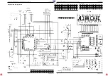
Page 18: ...2 4 0 2 4 0 2 57 2 7 2 42 2 4 2 45 PIN 59 60 61 62 80 0 2 52 2 5 2 4 IC802 MN151634 PIN 1 6 7 10 11 12 14 15 18 19 20 21 22 23 24 25 26 5 0 5 03 0 5 0 0 0 5 01 5 45 1 64 5 03 PIN 27 28 29 30 31 32 33...

Page 19: ...nabbildungen Circuit Diagrams and Layout of the PCBs Vertiga UMS 5100 Schaltpl ne und Platinenabbildungen Circuit Diagrams and Layout of the PCBs 3 14 3 13 Display Platte Display Board LED Platte LED...

Page 20: ...02 0 02 0 01 0 23 5 02 2 35 2 45 2 38 4 79 2 36 PIN 25 26 27 34 35 36 37 38 39 40 41 42 43 0 0 2 37 0 0 4 7 0 0 03 0 03 0 02 4 88 0 02 PIN 44 45 46 47 48 49 50 51 52 53 54 55 2 44 1 34 0 01 2 43 0 68...

Page 21: ...altpl ne und Platinenabbildungen Circuit Diagrams and Layout of the PCBs Vertiga UMS 5100 Schaltpl ne und Platinenabbildungen Circuit Diagrams and Layout of the PCBs 3 18 3 17 CD Platte CD Board IC403...

Page 22: ...g und Ersatzteilliste Exploded View and Spare Parts List Vertiga UMS 5100 Explosionszeichnung und Ersatzteilliste Exploded View and Spare Parts List Vertiga UMS 5100 Explosionszeichnung und Ersatzteil...

Page 23: ...DE 1 N 4001 GA D 00209 830921504500 DIODE 1N4148 AV619 GA D 00210 830921504500 DIODE 1N4148 AV619 GA D 00212 830921504500 DIODE 1N4148 AV619 GA D 00212 830921540100 DIODE 1N5401G GI FAG AV6 NETZTEIL P...

Page 24: ...SW 00007 759550489200 TAKTSCHALTER RS 014RB SW 00008 759550489200 TAKTSCHALTER RS 014RB SW 00009 759550489200 TAKTSCHALTER RS 014RB SW 00010 759550489200 TAKTSCHALTER RS 014RB SW 00011 759550324300 MI...

Reviews: