k
2 - 14
GRUNDIG Service
Description
TVR 3710 FR, TVR 5100 FR, TVR 5500 FR
On SP mode the DETAIL ENHANCER and on LP mode additionally the
NLE-stage is active. The NLE-stage is activated (at LOW level) via
IC7051-(25). The linear pre-emphasis (MAIN EMPH) which follows
increases the high-frequency components of the CVS signal linearly.
This preemphasis is reversed on playback mode to achieve a better
signal-to-noise ratio. The peripheral circuit for the non-linear network
consists of C2024 and R3012 (at pin 8), and for the linear network it is
made up of R3014, C2025, C2026, C2062 and R3013 (at pin 7). Via
IC7051-(7) the sync level (R3010) of the luminance signal is adjusted
at the MAIN EMPH stage. The white level cannot be changed. The
luminance signal is then fed to the FM Modulator in IC7051.
The frequency-modulated signal is fed out from pin 2 of IC7051 and is
taken via a low pass filter (T7010) to the junction R3023 / R3029 /
R3027 where it is added to the chroma signal. The sum signal (FMRV)
is passed through the amplifier stage T7018 / T7019 and plug contact
1902-(2) to the head amplifier.
Playback
On playback, the signal from the tape (FMPV) passes through plug
contact 1902-(9) to a few matching circuits for correction of the
frequency response and the delay time (C2043…T7014). Subse-
quently, the signal is fed through the emitter follower T7013 to Pin 1 of
the IC7051.
In IC7051, the signal path divides. For dropout identification, the signal
from the tape is supplied to the dropout detector (DO DET) which
produces a defined period pulse corresponding to the loss of level, to
the dropout compensation switch (DO). On another path, the signal is
fed through a limiting stage (DOUBLE LIM), a FM-demodulator, a
lowpass filter (SUB LPF), a deemphasis stage (MAIN DEEMPH)
containing a playback amplitude control, and an R/P-switch to pin 4 of
the IC7051. Afterwards, the CVS signal is passed through an amplifier
stage (T7007) and C2027 to IC7051-(5). In IC7051, the signal is
clamped (CLAMP) before and after the R/P-switch. After the lowpass
filter (Y-LPF) which follows the signal path divides. In one path, the
luminance signal is fed through a dropout switch and, after an R/P-
switch, leaves the IC7051 on pin 20. In the following delay circuit
(IC7060) the signal is delayed by one line and is then taken via
IC7051-(18) and the following amplifier stage (VCA) to the dropout
switch. If dropouts occur in the signal, the dropout switch changes over
replacing the faulty signal by the faultless delayed signal. In the other
path, the non-delayed and delayed CVS signals are subtracted in a
difference amplifier. The resulting low-frequency noise voltage is
added at opposite phase to the non-delayed Y-signal via a weighting
network. The noise-reduced Y-signal passes through the non-linear
deemphasis (NL DEEMPHASIS), the noise reduction stage (WHI NOI
CAN) for high-frequency noise voltages and a high-frequency preem-
phasis (PICTURE CONTROL). In the following "Y/C-MIX" stage the Y-
signal is added to the internally fed in chroma signal. The regenerated
CCVS signal is passed through an R/P-switch, the V-pulse insertion
stage (QH/QV INS, CHARA INS), a video amplifier (VIDEO AMP) and
is fed out from pin 16 of the IC7051. Subsequently, the CCVS signal
(VP) is taken to the "IN/OUT" circuit stage.
3.6.2 Signal Chassis – Chroma
"PAL/SECAM-BG"
Function Overview
On record the 4.43MHz chroma signal is converted to 627kHz with the
aid of a mixing frequency of 5.06MHz.
On playback the 627kHz chroma signal is reconverted into the original
4.43MHz chroma signal with the aid of the mixing frequency (5.06MHz).
The signal is amplified, added to the luminance signal and passed on
to the "IN/OUT" circuit stage.
Record
On record the signal path is the same for PAL and MESECAM (Secam
East). The CCVS signal (VR) is supplied from the "IN/OUT" circuit
stage to the IC7051 via pin 12. In this IC, the signal passes through the
Video-AGC-circuit, a -6dB-attenuator (1/2), an R/P-switch and an
integrated bandpass (FSC BPF). Here, the chroma signal is separated
from the CCVS signal. The chroma signal is then taken via two R/P-
switches, a gain controlled amplifier (ACC AMP) and a burst emphasis
stage (not active) to the main converter (MAIN CONV). In the main
converter, the chroma signal (4.43MHz) is mixed with the subcarrier
frequency (5.06MHz). In an internal lowpass filter unwanted mixing
products are eliminated from the converted chroma signal (627kHz).
Having passed the R/P-switch, the chroma lowpass filter (C-LPF) and
the colour killer which follow the signal arrives at pin 38 of IC7051. It is
then fed through an adjustment control for the chroma recording
current, R3029 (PAL CURR.) to the junction R3023 / R3029 where the
3.5 Signal Chassis – IN/OUT (IO)
General
The universal applicability of these video recorders requires special
facilities for distributing the input and output signals corresponding to
the operating mode. For this, the switching ICs IC7591, IC7592 and
IC7593 are necessary.
3.5.1 Input/Output Selection Switches
Selection and distribution of the signals is effected with switch-IC's.
The following switches are used according to the design of the
individual models:
– IC7591: Input selection switch (optional) for the TV Signal Electron-
ics. The TV input selection switch is supplied with the video and
audio signals from Tuner 1, from the EURO-AV socket, from the
Cinch-AV sockets (for camcorders), and the Video/Chroma and
Standard Sound stages.
– IC7592: Input selection switch for the Video/Chroma stage. The
VCR input selection switch is supplied with the video and audio
signals from Tuner 1 or 2, from the EURO-AV socket and the Cinch-
AV sockets (for camcorders).
– IC7593: Output selection switch for the EURO-AV socket (optional).
The EURO-AV output selection switch is supplied with the video and
audio signals from Tuner 1, Tuner 2, and from the TV input select
switch or the video part.
The signals are selected according to the operating mode and fed to
the circuit stages for Video/Chroma "VR", Standard Sound "AMLR",
TV signal processing "VTV" / "ATV", and the EURO-AV socket. The
switches are controlled by the deck computer IC7410 via the control
leads VS1 / VS2 for IC7591; RS1 / RS2 for IC7592; and OS1 / OS2 for
IC7593.
3.3.2 Decoder Operation
For financial and copyright reasons, a couple of independent television
stations transmit scrambled video and audio signals so that a Pay-TV-
Decoder is required to descramble the signals.
Technical realization
The Pay-TV-Decoder is to be connected to the EURO-AV socket.
When using the PAY-TV-Decoder, the coded video and audio signals
are taken via the EURO-AV socket to the Pay-TV-Decoder. The
Decoder descrambles the signals and feeds them back to the "IN/OUT"
circuit stage via the EURO-AV socket. This signal path must be
released on a per-programme basis when setting the programmes.
This signal path is released in TV mode by the switch IC's (IC7593 /
IC7591). In VCR mode, release is effected via the switch IC's (IC7593 /
IC7592).
3.6 Signal Chassis – Video/Chroma (VS)
Loop-through Signal Path (EE)
The CCVS signal (VR) selected in the "IN/OUT" circuit stage is fed to
pin 12 of IC7051. In this circuit, the signal passes through the VIDEO-
AGC-stage, an R/P-switch and, after the video amplifier (VIDEO AMP),
it is fed out from IC7051 on pin 16. Subsequently, the CCVS signal (VP)
is taken to the "IN/OUT" circuit stage.
3.6.1 Signal Chassis – Video
Function Overview
On record, the CCVS signal is processed and the luminance signal is
converted to a frequency-modulated signal in the video circuit stage.
On playback, the frequency-modulated signal obtained from the tape
passes through a demodulator, a dropout compensator, an equalizer
stage and the crispening stage. Thereafter, the CVS signal is added to
the chroma signal and fed to the "IN/OUT" circuit stage.
Record Signal Path
The CCVS signal (VR) selected in the "IN/OUT" circuit stage is fed from
pin 12 of the IC7051 to the Video-AGC-stage, then passes through a
-6dB attenuator (1/2), an R/P-switch, a clamping stage (CLAMP), a
lowpass filter (Y-LPF), and a few stages which are not active on record
mode. After the R/P-switch the signal is fed out from the IC7051 on Pin
4. At the base of the following amplifier stage T7007, a 4.43MHz trap
is provided for suppressing the chroma component of the CCVS signal.
The filtered out CVS signal is fed via an emitter follower (T7007) and
C2027 to IC7051-(5). In this IC, the signal is subjected to a clamping
stage, a DETAIL ENHANCER and the NLE-stage (non-linear empha-
sis).
Summary of Contents for TVR 3710 FR
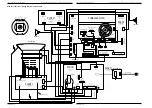
Page 16: ...Partie g n rale General Section TVR 3710 FR TVR 5100 FR TVR 5500 FR 1 16 GRUNDIG Service Notes...
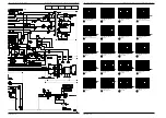
Page 91: ...TVR 3710 FR TVR 5100 FR TVR 5500 FR Vues clat es Exploded Views GRUNDIG Service E 3 3...
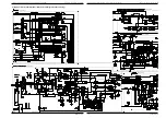
Page 92: ...Vues clat es Exploded Views TVR 3710 FR TVR 5100 FR TVR 5500 FR E 4 GRUNDIG Service 4...

