background image

2 - 16

GRUNDIG Service

Description

TVR 3710 FR, TVR 5100 FR, TVR 5500 FR

the "IN/OUT" circuit stage to the TV Signal Electronics and the EURO-
AV socket respectively.
On "LP" mode, switchover of the equalizing circuit is carried out by the
switch EP CTL.

3.7.4 Muting Circuit
The mute command (MTA) from the deck computer IC7410-(40) mutes
the audio outputs of IC7601 in all functions, with the exception of
playback and record, and also in the case of servo faults. For this, the
IC7601 obtains the mute command "MTA" via pin 22 (HIGH active).

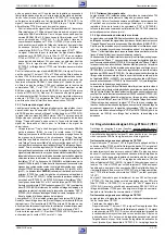
word corresponding to the brightness information and is present at
the output of the ROM after every 1

µ

s. This data word is entered into

a shift register and is read out at a 12MHz pixel clock derived from
the 6MHz clock. The corresponding R/G/B signals are available at
the push-pull outputs IC7880-(15…17). The maximum output level
of the R/G/B signals is determined by the voltage present on
IC7880-(18). The blank signal from IC7880-(19) is used to control
the insertion of the R/G/B signals in IC7200 within the TV Signal
Electronics (signal chassis).

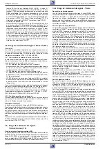
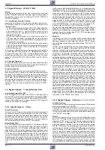
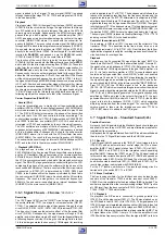
4. Teletext "DOS" (TXT)

Function Overview
The DOS unit contains a Test Pattern / Data Generator and the VPS/
PDC/Teletext processing stage with IC7881 or IC7880 (with VPS and
PDC processing) being the heart of it. The following description refers
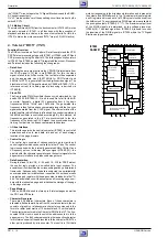
to IC7880. This IC7880, named IVT (Integrated Video-Input-Processor
and  Teletext) includes the following function groups:

– Data Slicer

The adaptive data slicer extracts the VPS/PDC/teletext data from
the CCVS signal (VTV) fed in via IC7880-(8). For this, the video
signal is taken to an A/D converter. The text data is then separated
and the appropriate clock (6.9375MHz for PDC/Teletext and
2.5MHz for VPS ) is generated from the digitised video signal. The
black level of the CCVS signal is stored by C2888 at IC7880-(7). The
reference current for analog signal processing is derived via
IC7880-(9).

– Clock-PLL

The free-running 27MHz oscillator frequency is determined by the
quartz Q1800 at IC7880-(2…4) and is used first of all for the A/D
converter. Secondly, a digital PLL generates from it the basic
frequencies 6MHz, 1MHz, and 15.625kHz. The generated line
frequency is then fed to a phase comparator along with the line sync
signals separated from the CCVS signal. The characteristic of the
digital loop filter which follows is influenced by a control register and
the 6MHz oscillator is controlled accordingly. By this method, all
frequencies generated in the IVT are synchronized to the line
frequency of the incoming CCVS signal. In unsynchronized condi-
tion (eg. test pattern) no phase comparison takes place.

– I

2

C-bus Interface

This interface permits the central computer (IC7880) to control all
operations and also to read data into and out of each storage
location of the page memory.

– Control Logic

The control logic consists of various counters, gate circuits and
control registers which can be controlled via the I

2

C-bus. The control

logic is supplied with the internally generated 6MHz, 1MHz, H and
V-frequency pulses. In this way, the sync signal (IC7880-(12)), the
pixel clock for the character generator, and the control signals for the
page memory interface are produced among others.

– Data Acquisition

During the lines 16 for VPS, 2…22 and 315…335 for PDC/Teletext
the control logic provides a so-called data input window. The
acquisition circuit identifies the corresponding data by a determined
frame code. Subsequently, the data is subjected to a serial/parallel
conversion and an error detection or correction. When the user calls
up a text page a register with the page number is loaded via the I

2

C-

bus. The acquisition circuit then compares all incoming page num-
bers with the requested page and initializes the storage of the page
in the page memory.

– Page Memory

The 8k x 8-DRAM is used to store up to 8 teletext pages as well as
the PDC and VPS data.

– Character Generator

There are 256 different characters. Each of these characters is
allocated a 8bit data word. Apart from 32 control characters, the set
consists of graphic or alphanumeric characters composed in the
form of a raster point matrix of 12 horizontal and 10 vertical points.
The characters are stored in the Character ROM in the IVT. The line-
coupled 1MHz clock is used to switch the addresses fed in to the
page memory. The 8bit code representing the respective character
in turn forms one part of the address fed in to the character ROM. The
other part is produced by a line counter. The result is a 12bit data

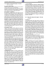
IC7880
SAA5281

Line Counters

and Display

Acquisition

Oscillator

/2

8k Memory

Character Generator Buffers
Character ROM

ODD/EVEN OR DV

Digital PLL

and processing

Sync separation

and Acquisition

Data slicing

AD-Conversion

Clamp

Control Registers

I2C Businterface

37

38

39

40

41

42

43

44

45

46

47

48

1

2

3

4

4

5

6

7

8

9

10

11

12

13

14

15

16

17

18

19

20

21

22

23

24

25

26

27

28

29

30

31

32

33

34

35

36

Summary of Contents for TVR 3710 FR

Page 1: ...00 00 PAL SECAM TVR 3710 FR TVR 5100 FR TVR 5500 FR TIMER 8 P RECORD 8 TIMER P RECORD TVR 3710 FR 77250 024 75 G CC 29 75 FB TVP 762 TVR 5100 FR 77250 034 75 G CC 33 75 FB TVP 762 TVR 5500 FR 77250 04...

Page 2: ...11 F Sommaire Page Partie g r rale 1 1 1 16 Composition des appareils 1 3 Appareils de mesure Moyens de maintenance 1 4 Caract ristiques techniques 1 4 El ments de commande 1 5 Tableaux des normes et...

Page 3: ...ad Amplifier OHA 27599 004 07 S P 4 69 Ampli de t tes Head Amplifier OHA 27599 004 08 CCIR B G H PAL CCIR I PAL CCIR B G L L SECAM NTSC Lecture NTSC Playback 2 Etages de r ception Frontend 2 Tuner Dia...

Page 4: ...ptateur pour couplem tre 600gf cm 75987 262 73 Tournevis de r glage 75987 262 80 Pointe mandrin de r glage de tension de bande 75988 002 27 Extracteur de tambour de t tes 75988 002 37 Gants de nylon d...

Page 5: ...e en position Stop R Lecture p Recherche visuelle avant en lecture avance rapide en position Stop r Termine toutes les fonctions stop Ejection de la cassette V Volume P S lectionne la cha ne l ments d...

Page 6: ...ce par la touche secteur Exemple Appelez le tableau INFOCENTER avec la touche h S lectionnez la ligne INSTALLATION l aide des touches et appelez avec la touche G S lectionnez la ligne CLASSER NUMERO P...

Page 7: ...Hz 519 25MHz 527 25MHz 535 25MHz 543 25MHz 551 25MHz 559 25MHz 567 25MHz 575 25MHz 583 25MHz 591 25MHz 599 25MHz 607 25MHz 615 25MHz 623 25MHz 631 25MHz 639 25MHz 647 25MHz 655 25MHz 663 25MHz 671 25M...

Page 8: ...63 25MHz 671 25MHz 679 25MHz 687 25MHz 695 25MHz 703 25MHz 711 25MHz 719 25MHz 727 25MHz 735 25MHz 743 25MHz 751 25MHz 759 25MHz 767 25MHz 775 25MHz 783 25MHz 791 25MHz 799 25MHz 807 25MHz 815 25MHz 8...

Page 9: ...cturetubepanel to the metal screen Fig 2 Operating the TVR with the Power Chassis removed Place the Power Chassis behind the set as shown in Fig 5 Re connect the plug connections Attention The Power C...

Page 10: ...t de montage suffisamment vers le fond de l appareil pour que le contact 1918 Fig 7 soit accessible sur le C I de traitement du signal D faire le contact 1918 du C I de traitement du signal D faire le...

Page 11: ...er les 2 vis Pos 12 Fig 11 Pousser le C I de traitement du signal dans le sens de la fl che Fig 11 et retirer celui ci par le haut Kabeladapter Extension cable kit Sach Nr part no 75988 009 79 Fig 10...

Page 12: ...NS ACCELERATING VOLTAGE MAX 25KV 0 8mA FLA VE SHOW VIEW IS A TRADEMARK APPLIED FOR BY GEMSTAR DEVELOPMENT CORP SHOW VIEW SYSTEMS IS MANUFACTURED UNDER LICENSE FROM GEMSTAR DEVELOPMENT CORPORATION Code...

Page 13: ...urs du niveau de maintenance SERVICE STATUS Service Test Programme Calling up Checking the Levels of and Terminating the Service Test Programme The service test programme must not be called up from th...

Page 14: ...econtraste laluminosit lereliefdel image lasaturationde la couleur et le volume restent charg es Appel des fonctions d effacement A l aide des touches de la t l commande s lectionner la ligne RAM CLEA...

Page 15: ...nd tuner 1301 for video signal recording Repair tip With the tuner selection function it is possible to feed picture and sound of tuner 1301 into the TV signal path and to play these signals back Acti...

Page 16: ...Partie g n rale General Section TVR 3710 FR TVR 5100 FR TVR 5500 FR 1 16 GRUNDIG Service Notes...

Page 17: ...nversion de la polarit des tensions au transformateur un courant circule dans les enroulements secondaires travers les diodes les condensateurs et la charge Si l ensemble de l nergie accumul e dans le...

Page 18: ...on dispo nible C2551 Si le courant de faisceau d passe 1mA la tension devientn gative Apartird env 18VlesdiodesD6550 D6552 devien nent conductrices et la tension 1923 2 chute 1 5V la THT est trop lev...

Page 19: ...bande d livrent des impulsions lorsqu ils reconnaissent le d but ou la fin de la bande magn tique Les tensions de sortie des phototransistors sont appliqu es aux entr es analogiques du P IC7410 55 57...

Page 20: ...D codage des signaux de t l commande par le r cepteur infra rouge IC7812 Horloge quartz RAM int gr e pour la m morisation des donn es Timer Commande des diodes lectroluminescentes Timer Enregis tremen...

Page 21: ...aitement du signal vid o Le s lecteur d entr e de l tage de traitement du signal vid o Lumi nance Switch re oit d une part l IC7200 13 le signal vid o compo site FBAS en provenance de l tage FI et d a...

Page 22: ...en fr quence En lecture le signal FM en provenance de la bande traverse les tages d modulateur compensation drop out d saccentuation et contours Ensuite le signal BAS de luminance est additionn au sig...

Page 23: ...de la fr quence ligne 321fH Cela correspond une fr quence de 5 015625MHz Dans un compteur 1 2 et un r gulateur de phases 1 4 la fr quence est divis e par 8 puis est dirig e vers le m langeur interm di...

Page 24: ...Lepointfroiddelat teE Lsonestreli la masse depuis 1901 3 R3600 et l IC7601 2 Le r glage de la pr magn tisation se fait par R6318 BIAS Dans le cas d enregistrement LP la commutation de correction d enr...

Page 25: ...D IC7310 3 T7330 T7330 current flows through the secondary windings of the transformer through the diodes electrolytic capacitors into the load When the whole amount of energy stored in the transforme...

Page 26: ...us causing the voltage at plug contact 1923 2 to decrease to 1 5V is mainly determined by the diodes D6553 D6556 D6554 and R3554 The triggering threshold for the safety circuit depends on the screen s...

Page 27: ...and the identifi cation TAS for the beginning of the tape and TAE for the end of the tape The threading tachopulses FTA are supplied to the C via plug contact 1905 11 and IC7411 5 15 FTAD The tape dec...

Page 28: ...7870 The drifting of tuner 1 or of the aerial signal produces the AFC1 control voltage in the Frontend circuit of the TV Signalelectronic This voltage is supplied to pin 24 and the keyboard control co...

Page 29: ...ted R G B signals pass through the R G B selection switch Clamp Switch In the output stage the R G B signals are controlled in brightness BRI via pin 17 and in contrast CONTR via pin 25 Automatic cont...

Page 30: ...C AMP and a burst emphasis stage not active to the main converter MAIN CONV In the main converter the chroma signal 4 43MHz is mixed with the subcarrier frequency 5 06MHz In an internal lowpass filter...

Page 31: ...ilter circuit Q5103 Subsequently the signal passes through a 15dB amplifier and is then taken via pins 25 and 24 to a limiting amplifier with a following frequency divider Dividing the chroma signal i...

Page 32: ...by a control register and the 6MHz oscillator is controlled accordingly By this method all frequencies generated in the IVT are synchronized to the line frequency of the incoming CCVS signal In unsyn...

Page 33: ...ignements Adjustment Procedures Sch ma des points de r glage Location of Adjustment Controls 1 C I Alimentation T H T Power Chassis PLSP Ubat 1 v shift v amp 3358 5550 1925 5551 3523 3524 FOCUS SCREEN...

Page 34: ...ignal Signal Chassis PSSP2 1701 1702 1 9 1 5 1 3 0 1 CLOCK SYNC FREQU SECAM CURR PAL CURR AGC1 L ADJ1 BIAS PB LEVEL AFC2 AGC2 TDA9812 L ADJ2 TDA9800 PHASE H SHIFT 2814 3010 3029 3027 3712 3729 3606 36...

Page 35: ...s l aide des r glages R3920 RED Cutoff R3918 GREEN Cutoff et R3917 BLUE Cutoff R gler R3919 GREEN Gain et R3921 BLUE Gain de fa on obtenir une image sans dominante de couleur dans la zone des gris 2 C...

Page 36: ...du CAG HF du tuner R3341 AGC2 3 5 Etage de traitement du signal Vid o Chroma VS Appareil et moyens de mesure Cassette vide Oscilloscope avec sonde 10 1 Fr quencem tre G n rateur de mire couleur R glag...

Page 37: ...n OSD scale Brightness 50 Screen grid adjustment control SCREEN left stop R3919 R3921 center position Feed a black test pattern into the AV socket With the cutoff controls R3920 R3918 and R3917 set th...

Page 38: ...counter connector contact 1902 2 Connect IC7051 2 via 150 and 22 H to 5V supply Oscilloscope connector contact 1902 2 Feed in a PAL red raster test pattern with 75 saturation into the AV socket and re...

Page 39: ...1 RFK 1 G 8V R GNDTV B 1 2 3 MEH2 MEH1 N C 1 2 3 LS1 N C LS2 RFK 5 RFK 5 1911 HFB 5 1 2 3 4 HDR GNDTV VFB VDR 7V 9A 6 5 1 2 3 4 GND9A VCOMP BCI PROT 3 2 1 TMO1 N C TMO2 5 1 2 3 4 PG FG 14M2 GNDD GNDM...

Page 40: ...7 5 1 2 3 4 GND9A VCOMP BCI PROT 3 2 1 TMO1 N C TMO2 5 1 2 3 4 PG FG 14M2 GNDD GNDM2 5D 6 REEL 15 11 12 13 14 FTA WTR LED INIT TAS 5 1 2 3 4 GNDM1 FG CAP CREV 14 9 10 6 7 8 9 GNDD TAE 5STBY WTL RECP 1...

Page 41: ...1 2 3 4 GND9A VCOMP BCI PROT 3 2 1 TMO1 N C TMO2 5 1 2 3 4 PG FG 14M2 GNDD GNDM2 5D 6 REEL 15 11 12 13 14 FTA WTR LED INIT TAS 5 1 2 3 4 GNDM1 FG CAP CREV 14 9 10 6 7 8 9 GNDD TAE 5STBY WTL RECP 1 3 7...

Page 42: ...TVR 3710 FR TVR 5100 FR TVR 5500 FR Circuits imprim s et sch mas lectriques Layout of PCBs and Circuit Diagrams TVR 3710 FR TVR 5100 FR TVR 5500 FR Synoptique des circuits imprim s Block Circuit Diagr...

Page 43: ...200 29 TV 35 AC 200mV Div 20 s Div IC7200 28 TV 36 DC 500mV Div 20 s Div 0V IC7200 20 TV 37 DC 500mV Div 20 s Div 0V IC7200 19 TV 38 DC 500mV Div 20 s Div 0V IC7200 18 TV 39 DC 500mV Div 10 s Div 0V T...

Page 44: ...5500 FR Circuits imprim s et sch mas lectriques Layout of PCBs and Circuit Diagrams TVR 3710 FR TVR 5100 FR TVR 5500 FR Synoptique des circuits imprim s Block Circuit Diagram Video Analog 4 11 GRUNDIG...

Page 45: ...itter REC 3 AC 500mV Div 200 s Div IC7608 7 REC 8 AC 200mV Div 200 s Div IC7608 7 PB 8 AC 100mV Div 200 s Div IC7601 11 REC 9 AC 500mV Div 200 s Div IC7601 17 REC 10 AC 20V Div 5 s Div C2618 REC 11 AC...

Page 46: ...00mV Div 500ms Div 0V Connector 1905 9 12 IC7411 6 7 REC 16 DC 100mV Div 5ms Div 0V Connector 1905 13 REC 17 DC 1V Div 10ms Div 0V Connector 1901 7 REC 18 DC 500mV Div 500 s Div 2 8V Connector 1905 2...

Page 47: ...m s et sch mas lectriques Layout of PCBs and Circuit Diagrams DC 1V Div 10ms Div 0V Connectors 1904 1 1930 6 REC 23 Reference AL P 4 65 BUPI P 4 68 CO P 4 43 DE P 4 49 IO P 4 59 OHA P 4 69 PLSP P 4 19...

Page 48: ...triques Layout of PCBs and Circuit Diagrams TVR 3710 FR TVR 5100 FR TVR 5500 FR C I Interruptur secteur Power Switch Board Vue c t composants View of Component Side 1 2 3 1 2 3 B A B A 1 0 0 2 B 2 1 0...

Page 49: ...7 35 0 B 7 7 35 1 A 8 7 35 2 D 6 7 51 0 G 11 7 55 0 I 10 7 57 8 I 11 7 58 3 D 9 7 58 4 A 9 7 58 5 E 9 7 58 6 F 9 7 58 7 A 9 9 30 1 C 5 9 30 2 C 6 9 30 3 C 3 9 30 4 B 5 9 30 5 F 5 9 30 7 H 4 9 30 9 B...

Page 50: ...337 BYT54 6336 1N5062 6316 1N5062 6314 1N5062 6313 1N5062 6315 BAV21 6335 BYD33D 6334 BYT54 6332 BYV10 20 6348 100u 2335 68u 2315 2u2 2320 5331 1 3 4 5 6 7 2 8 STP4NA60FI 7330 DMF 2830 5311 1300 T2 5A...

Page 51: ...343 L16 6337 I 9 6336 H 9 6335 K 9 6334 J10 6332 F10 6316 C10 6315 C10 6314 C 9 6313 C 9 5590 B27 5580 F22 5556 M32 5550 B31 5374 J16 5373 F15 5372 E16 5371 E16 5370 F14 5366 E15 5365 D13 5364 H16 536...

Page 52: ...332 BYD33D 6334 BAV21 6335 1N5062 6315 1N5062 6313 1N5062 6314 1N5062 6316 BYT54 6336 BYT54 6337 2u2 2320 68u 2315 100u 2335 5330 1 3 4 5 6 7 2 8 STP4NA60FI 7330 DMF 2830 5311 1300 T2 5AH 1311 3310 1...

Page 53: ...15 6372 G14 6371 F14 6361 E14 6351 J14 6348 I 7 6343 M16 6337 I10 6336 I10 6335 L 9 6334 J10 6332 F10 6316 D10 6315 C10 6314 C10 6313 D10 5581 G22 5556 M32 5550 B31 5510 C22 5374 J16 5373 G15 5372 F16...

Page 54: ...1N5062 6314 1N5062 6313 1N5062 6315 BAV21 6335 BYD33D 6334 BYT54 6332 BYV10 20 6348 100u 2335 68u 2315 2u2 2320 5330 1 3 4 5 6 7 2 8 STP4NA60FI 7330 DMF 2830 5311 1300 T2 5AH 1311 3310 1 2 3 1013 101...

Page 55: ...0 J16 7331 D15 7330 G 9 7310 G 5 6592 H33 6584 K32 6583 G21 6582 D23 6581 K32 6556 K28 6555 F34 6554 L28 6553 J28 6552 K31 6551 K31 6550 L31 6513 K22 6393 I15 6392 H14 6374 K14 6373 G15 6372 G14 6371...

Page 56: ...04 100n 2906 10n 2907 6906 BAV21 2k2 3921 2k2 3919 470E 3920 470E 3917 470E 3918 1961 4454 S 6 8 4 5 2 10 1 TDA6103Q N2 7900 1 2 3 4 5 6 7 8 9 1962 1969 1 2 3 4 1967 1 2 3 4 5 1 2 3 4 5 1 2 3 4 5 D C...

Page 57: ...PCB 1925 SCREEN B Gain G Gain 1920 TO POWER PCB 1926 ANODE L5550 1924 TO POWER PCB FOCUS TO FAMILYBOARD 1913 R G B 8 GNDTV HEATER GNDA AQUADAG VRGB DEG1 DEG2 TO POWER PCB Uref B Cutoff G Cutoff R Cut...

Page 58: ...1 50 9 1 9 8 9 2 1 9 9 2 2 0 9 2 2 1 9 2 2 2 9 2 2 3 92 25 92 26 9 0 4 2 9 0 4 3 9 0 4 4 90 73 9 1 1 1 9 1 1 2 91 14 9 11 8 9 12 3 9 1 4 2 5 4 0 1 588 2 6 8 0 1 2 8 0 1 3 4 3 6 9 0 9 9 9 1 0 1 91 02 9...

Page 59: ...811 J 4 3816 H 4 3822 H 5 3823 H 2 3824 J 4 3825 H 2 3829 H 3 3830 H 4 3831 H 4 3835 F 1 3838 I 4 3853 C 1 3868 D 1 3869 D 1 3878 G 1 3879 G 1 3898 G 2 5000 D 9 5001 A 4 5002 D 8 5003 B 6 5004 C 7 500...

Page 60: ...E 2 3476 E 2 3477 G 13 3480 E 11 3481 E 11 3482 E 11 3483 D 12 3484 E 11 3485 D 11 3486 D 11 3487 D 11 3488 D 11 3489 E 11 3490 E 2 3491 E 3 3492 E 2 3493 E 12 3496 E 12 3500 I 14 3501 I 14 3502 I 14...

Page 61: ...3 3 2 2 8 3 7 1 8 3 7 4 7 3 7 5 0 3 7 5 3 273 2 2 8 0 9 2 2 2 5 2 2 2 6 2 7 2 9 75 91 7 593 7 5 0 2 7 5 0 7 4 0 5 5 4 073 4 0 9 4 4 0 9 5 4 0 9 9 4 1 1 9 4 2 0 4 4 2 1 1 7 5 0 1 35 42 40 51 4 0 5 2 4...

Page 62: ...4k7 3826 4k7 3824 100E 3822 2k2 3816 6k8 3813 39k 3800 150k 3808 100 382 3k3 3834 3k3 3833 10k 3867 10k 3865 10k 3866 10k 3836 220E 3835 10k 3829 100k 3801 10 382 4k7 3830 100E 3831 0E 4084 4k7 3832 1...

Page 63: ...3827 G15 7870 B19 7870 A20 7870 B20 7870 A23 7861 K10 7860 K 9 7840 B 6 7820 H22 7813 E 5 7812 B 8 7811 A 8 7805 A10 7801 C13 6869 I 5 6868 I 6 6863 K 6 6862 K 6 6861 J 6 6860 J 7 6830 J10 6805 H19 6...

Page 64: ...04 F 9 7102 A 6 6103 H 8 3602 F 9 3601 E 8 3500 K 8 3600 D 9 3502 K 8 3501 J 8 3300 E 6 3202 E 5 3201 E 5 3200 E 5 1969 I10 1967 K 2 1965 G 2 1604 C 8 4 5 6 7 8 9 10 2 3 L K J I H G F E D C B M L K J...

Page 65: ...M 8 3488 M 8 3487 M 8 4 5 6 1 7 8 9 10 11 12 13 14 15 16 17 2 18 19 20 21 22 3 M L K J I H G F E D C B A O N M L K J I H G F E D C B A O N 4 5 6 1 7 8 9 10 11 12 13 14 15 16 17 2 18 19 20 21 22 3 5ST...

Page 66: ...8 5201 GNDTV GNDTV GNDD GNDD GNDTV GNDTV GNDTV GNDTV GNDTV GNDTV GNDTV GNDAM GNDAM GNDAM GNDAM GNDD GNDD GNDTV GNDTV GNDTV GNDTV GNDTV GNDTV GNDTV GNDTXT GNDTXT GNDTXT GNDTXT GNDD GNDD GNDD GNDD GNDD...

Page 67: ...1 3741 J 1 3740 K 8 3738 K 8 3737 K 8 3736 L 8 3735 K13 3734 L 9 6206 L21 3733 K10 3732 L11 3731 M 9 3730 M10 3729 M10 3728 N11 3727 K11 3725 K12 3720 L13 3719 D 8 6205 N32 3718 M14 3716 K13 3715 C13...

Page 68: ...12 13 14 15 16 17 2 3 2327 100p 1n 2331 2315 220p 100n 2333 50V 100n 2303 100n 2302 100n 2309 100n 2325 220n 2307 8p2 2308 100n 2306 2317 10n 1n 2304 220p 2332 120p 2328 2330 2329 2313 47p 2314 47p 1...

Page 69: ...2 2306 C11 5307 K14 2304 D 7 2303 J 3 2302 J 2 2301 F 1 2300 C11 1501 I 1 1346 I15 1345 J15 1340 K14 1324 G 9 5305 F 7 1322 D 9 1320 F 8 1301 G 4 7308 C16 5304 J18 5303 C13 5302 G 5 5301 F 7 5300 J 2...

Page 70: ...T GNDTXT GNDTXT GNDTXT GNDTXT GNDTXT GNDTXT GNDTXT GNDTXT GNDTXT GNDTXT 2894 2893 100n 2887 10p 2884 100n 2890 100n 2888 1n 2885 100n 2889 100n 2882 100n 2886 100n 2880 15p 2883 100n 2891 3799 0E 3897...

Page 71: ...3 6512 G 5 6510 F12 6509 F13 6508 F14 4 5 1 6 7 8 9 10 11 12 13 14 15 16 2 3 H G F K E D C B A J I H G F K E D C B A J I 4 5 1 6 7 8 9 10 11 12 13 14 15 16 2 3 BC848B 7505 BC848B 7504 BC848B 7500 BC84...

Page 72: ...n 2068 1n 2067 10n 2064 10n 2066 100n 2042 2 2026 390p 10n 2010 10n 2075 100n 2073 10n 2012 1n 2071 33p 2118 2117 1n 2 2 68p 2033 10p 2034 2 2 200p 2032 10p 2031 10n 2028 10n 2014 47p 2045 470p 2076 G...

Page 73: ...B25 7101 A28 7100 B30 7070 A18 7060 M20 7051 H 6 7021 O 6 7020 N 4 7019 D 3 7018 C 4 7016 J 2 7015 I 2 7014 O 9 7013 N10 7010 I 6 7009 P 2 7007 K 8 7006 N25 7005 M10 7003 C12 7002 B12 7001 L13 7000 B...

Page 74: ...01 E10 6694 C15 6693 C15 6692 B15 6691 A14 6690 A13 4 5 6 7 1 8 9 10 11 12 13 14 15 16 2 3 H G F K E D C B A J I H G F K E D C B A J I 4 5 6 7 1 8 9 10 11 12 13 14 15 16 2 3 10E 3661 68k 3660 10E 3622...

Page 75: ...32 73 6 274 6 275 327 6 2 2 7 0 AC 500mV Div 200 s Div IC7608 7 REC 8 AC 200mV Div 200 s Div IC7608 7 PB 8 AC 100mV Div 200 s Div IC7601 11 REC 9 AC 500mV Div 200 s Div IC7601 17 REC 10 AC 20V Div 5...

Page 76: ...B A E D C B A 0006 A 2 0006 0 0 07 1910 C 3 1911 B 1 1912 B 1 1920 D 3 1930 D 3 1931 D 1 2026 C 2 2106 C 2 2303 E 1 2304 E 1 2305 E 1 2314 E 2 5002 C 3 5101 D 3 5301 D 3 7301 E 2 7302 E 3 9 10 1 1 1...

Page 77: ...G F K E D C B A J I 4 5 1 6 7 8 9 10 11 12 13 14 15 16 2 3 2021 100n 22n 2014 10n 2010 10n 2011 10p 2012 10n 2005 10n 2006 10n 2008 10n 2007 10n 2004 220p 2103 22p 2101 22n 2009 10n 2003 10n 2002 10n...

Page 78: ...a main sans cassette D brancher l appareil du secteur D gager les verrous R Fig 1 et S Fig 2 du logement de cassette tout en poussant celui ci suffisamment vers l int rieur jusqu ce qu il commence l g...

Page 79: ...rous R Fig 1 et S Fig 2 du logement de cassette tout en poussant celui ci suffisamment vers l int rieur jusqu ce qu il commence l g rement descendre Tourner le moteur de chargement dans le sens engage...

Page 80: ...e la m canique Courroie d entra nement Pos 126 poulie Pos 128G et C I cap teurs de m canique d mont s Bottom of Drive Mechanism Capstan belt Pos 126 pulley Pos 128G and sensor print assembly removed R...

Page 81: ...rn the lever by 90 in the direction of the arrow OPEN and remove the headwheel together with the lower clamping element Fig 10 Fig 7 A B 2 3 Le tambour de t tes Remarque Pour le d montage du tambour d...

Page 82: ...ignements chap 3 R glage du courant d enregistrement voir alignements chap 3 Contr le du d filement de bande voir point 3 1 Installation Before fitting the new headwheel make sure that the motor spind...

Page 83: ...che et retirer le moteur de chargement Pos 38 de son support Fig 15 Lors du montage veiller ce que le moteur soit bien enclench dans les supports avant et arri re 2 6 Le moteur cabestan Pos 127 Amene...

Page 84: ...Left Pos 23 Set the tape deck to the Eject position Unhook the tension arm spring pos 11 to avoid the tension arm spring being pre loaded At the bottom side of the tape deck partially unhinge the sen...

Page 85: ...0 et retirer le C I capteurs de m canique Apr s le remontage de l ensemble C I capteurs de m canique faire enclencher les crochets clip et fixer le verrou plastique A Remarque Diff rentsC I capteursde...

Page 86: ...de chargement gauche et droit Pos 23 et Pos 26 l aide du tournevis de r glage r gler le signal de suivi de piste TRIV de fa on le rendre aussi plat que possible avec l amplitude la plus forte Fig 24 A...

Page 87: ...ment de plusieurs l ments du chemin de bande il peut tre n cessaire de r p ter plusieurs reprises les r gla ges des points 3 1 1 et 3 1 2 3 2 Le r glage de la distance X Avant de proc der ce r glage l...

Page 88: ...tdroitetletourner dans le sens inverse des aiguilles d une montre jusqu ce que le plateau d enroulement patine l g rement Fig 28 La valeur affich e par le couplem tre doit tre de 7mNm 3mNm 70gf cm 30g...

Page 89: ...3 34 35 24B 23 26 22M 140 20R 20aR 13R 19R 18R 17R 25B 27B 28M 31Q 32Q 30Q 18R 15 14P 6P 6P 10P 11 12 2 5P 150 48S 44BS 42P 45S 36 37 38 39 40M 41S 46S 47 2 1 13R 49M 9 27B Exploded Views and Spare Pa...

Page 90: ...R TVR 5100 FR TVR 5500 FR E 2 GRUNDIG Service 2 126 114 120M 117 I 116 I 115 113B 118 112M 111B 106 105L 104L 101L 102L 127 128I 129 Option 125M 103L Graisse Grease R f N Part No 75988 002 36 Isopropa...

Page 91: ...TVR 3710 FR TVR 5100 FR TVR 5500 FR Vues clat es Exploded Views GRUNDIG Service E 3 3...

Page 92: ...Vues clat es Exploded Views TVR 3710 FR TVR 5100 FR TVR 5500 FR E 4 GRUNDIG Service 4...

Page 93: ...EXIBLE LEITUNG 1971 1935 3P CABLE EN NAPPE 1971 1935 3P 8018 000 75988 017 20 FLEXIBLE LEITUNG 1918 1937 4P CABLE EN NAPPE 1918 1937 4P 72010 524 77 BEDIENUNGSANLEITUNG F MODE D EMPLOI F 72010 525 00...

Page 94: ...i ces d tach es D Btx 32700 4 96 LEISTUNGS CHASSIS PLSP14B CHASSIS ETAGE DE PUISSANCE PLSP14B LEISTUNGS CHASSIS BILDROHRPLATTE BUCHSENPLATTE CHASSIS ETAGE DE PUISSANCE C I TUBE C I EMBASES POS NR ABB...

Page 95: ...SSIS BILDROHRPLATTE NETZSCHALTERPLATTE BUCHSENPLATTE CHASSIS ETAGE DE PUISSANCE C I TUBE C I INTERRUPTEUR SECTEUR C I EMBASES BEZEICHNUNG REFERENCE SACHNUMMER DESIGNATION POS NR N POS BEZEICHNUNG REFE...

Page 96: ...DIODE BZX 79 C 18 D 6261 8309 198 542 DIODE BAT42 43 BAT85 86 D 6262 8309 198 542 DIODE BAT42 43 BAT85 86 D 6263 8309 198 542 DIODE BAT42 43 BAT85 86 D 6280 8309 720 112 Z DIODE 12 C 0 5W D 6500 8309...

Page 97: ...008 20 QUARZ 10 MHZ Q 1745 75990 200 56 QUARZ SFE 5 5MHZ Q 1800 75988 032 57 QUARZ 27 MHZ HC49 UA Q 1801 75988 028 25 QUARZ 8 MHZ Q 1803 75988 005 01 QUARZ 32 768 KHZ R 3010 75988 009 41 TRIMMER 10KOH...

Page 98: ...B T 7708 8301 004 848 SMD TRANS BC 848 B T 7709 75988 010 36 TRANS DTC 124 EK T 7711 75988 010 36 TRANS DTC 124 EK Ersatzteilliste Pi ces d tach es D Btx 32700 4 96 SIGNAL CHASSIS PSSPG1 GLPVTF ETAGE...

Page 99: ...RKER FIXATION AMPLIDE TETES 0022 000 1 75988 018 11 M TRAEGER EQUERRE DE FIXAT 0023 000 1 75988 001 07 FAEDELSCHLITTEN LINKS CHARIOT DE CHARGEMENT GAUCHE 0024 000 1 75988 001 25 B LADEARM LINKS LEVIER...

Page 100: ...68 GRUNDIG ITALIANA S P A Via G B Trener 8 Trento 00 39 461 89 31 11 GRUNDIG SVENSKA AB Albygatan 109 d Box 4050 Solna 00 46 8 6 29 85 30 GRUNDIG DANMARK A S Lejrvej 19 V rl se 00 45 42 48 68 22 SF 02...

Reviews: