GV-395 Virtex-II DSP Hardware Accelerator Manual
GV & Associates, Inc.
07/10/04
42
13.5
GVA-DA9772 125 MSPS 14 Bit D/A
The DA9772 is a current-output DAC with a nominal full-scale output current of 20 mA and > 100 k output
impedance support update rates up to 125 MSPS. Differential current outputs are provided to support single-ended
or differential applications. Matching between the two current outputs ensures enhanced dynamic performance in a
differential output configuration. The current outputs may be tied directly to an output resistor to provide two
complementary, single-ended voltage outputs or fed directly into a transformer. The output voltage compliance
range is 1.25 V.
13.5.1
Single-Ended Output Path
A single-ended output is suitable for applications requiring a unipolar voltage output. A positive unipolar output
voltage will result if IOUTA and/or IOUTB is connected to an appropriately sized loDA resistor, 51-ohm, referred
to ACOM. This configuration may be more suitable for a single-supply system requiring a dc coupled, ground
referred output voltage. The DA9772 can be configured to provide a unipolar output range of approximately 0 V to
+0.5 V for a doubly terminated 50 cable since the nominal full-scale current 20 mA flows through the equivalent
RLODA of 25 ohm . In this case, RLODA represents the equivalent loDA resistance seen by IOUTA or IOUTB.
The unused output (IOUTA or IOUTB) can be connected to ACOM directly or via a matching 25-ohm resistor.
13.5.2
Differential Coupled Analog Output Path
An RF transformer is be used to perform a differential-to-single-ended signal conversion. A differentially coupled
transformer output provides the optimum distortion performance for output signals whose spectral content lies
within the transformer’s passband. An RF transformer such as the Mini-Circuits T1-1T provides excellent rejection
of common-mode distortion (i.e., even-order harmonics) and noise over a wide frequency range. It also provides
electrical isolation and the ability to deliver twice the power to the loDA. Note that the transformer provides ac
coupling only.
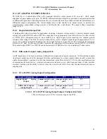
13.5.3
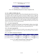
GVA-DA9772 Analog Output Configuration
Output Configuration
JP2
JP3
Output Connector
Singled-Ended Analog
Output
Jumper on pin 1 and
pin 2
Jumper on pin 1 and
pin 2
P1
Differential Coupled
Analog Output
Jumper on pin 2 and
pin 3
Jumper on pin 2 and
pin 3
P2
13.5.3.1
GVA-DA9772 Analog Output Jumper Configuration Table
* Pin 1 is the closest pin to GV & Associates logo on the PCB.
13.5.4
GVA-DA9772 PLL Configuration
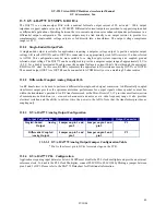
Applications requiring input data rates below 6 MSPS must disable the PLL clock multiplier and provide an external
reference clock . To disable the PLL Clock Multiplier, connect PLLVDD to PLLCOM by DAding a jumper between
pins 2 and 3 of JP1. Please refer to the DA9772 Data sheet for DAditional information.

