GV-395 Virtex-II DSP Hardware Accelerator Manual
GV & Associates, Inc.
07/10/04
23
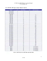
10.5
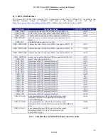
DP USB Interface
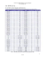
The Cypress CY7C68001 USB Controller (U19) is connected to both Virtex-II FPGAs (U14). An software and
firmware interface design is available. The link to the design on our web site is
(
http://www.gvassociates.com/software.asp?prod=12
). Additional documentation is also available.
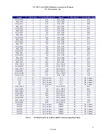
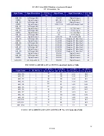
Signal Name
Signal Description
DP FPGA (U14) Pin No.
USB0_SLRD
read strobe for the slave FIFOs connected to FDI[15..0]
AK34
USB0_SLWR
write strobe for the slave FIFOs connected to FDI[15..0]
AF27
USB0_SLOE
output enable for the slave FIFOs connected to FD[15..0]
AG28
USB0_READY
ready that gates external command reads andwrites. Active
High.
USB0_INT
external interrupt signal. Active Low.
USB0_FIFOADR2 address bus select for the slave FIFOs connected to FD[15..0]
AF30
USB0_FIFOADR1 address bus select for the slave FIFOs connected to FD[15..0]
AG30
USB0_FIFOADR0 address bus select for the slave FIFOs connected to FD[15..0]
AE29
USB0_PKTEND
packet end signal for the slave FIFOs connected to FD[15..0]
AF29
USB0_CS# master
chip
select (active low)
AE27
USB0_FD15
Bidirectional FIFO/Command Data Bit 15
AG31
USB0_FD14
Bidirectional FIFO/Command Data Bit 14
AF31
USB0_FD13
Bidirectional FIFO/Command Data Bit 13
AG32
USB0_FD12
Bidirectional FIFO/Command Data Bit 12
AF32
USB0_FD11
Bidirectional FIFO/Command Data Bit 11
AB25
USB0_FD10
Bidirectional FIFO/Command Data Bit 10
AC25
USB0_FD9
Bidirectional FIFO/Command Data Bit 9
AH33
USB0_FD8
Bidirectional FIFO/Command Data Bit 8
AJ33
USB0_FD7
Bidirectional FIFO/Command Data Bit 7
AD32
USB0_FD6
Bidirectional FIFO/Command Data Bit 6
AE31
USB0_FD5
Bidirectional FIFO/Command Data Bit 5
AC27
USB0_FD4
Bidirectional FIFO/Command Data Bit 4
AD27
USB0_FD3
Bidirectional FIFO/Command Data Bit 3
AH34
USB0_FD2
Bidirectional FIFO/Command Data Bit 2
AJ34
USB0_FD1
Bidirectional FIFO/Command Data Bit 1
AD30
USB0_FD0
Bidirectional FIFO/Command Data Bit 0
AE30
USB0_FLAGA
a programmable slave-FIFO output status flag signal.
Defaults to PRGFLAG for the FIFO selected by the
FIFOADR[1:0] pins
AE26
USB0_FLAGB
a programmable slave-FIFO output status flag signal.
Defaults to FULL for the FIFO selected by the FIFOADR[2:0]
pins.
AD26
USB0_FLAGC
a programmable slave-FIFO output status flag signal.
Defaults to EMPTY for the FIFO selected by the
FIFOADR[2:0] pins.
AE28
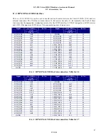
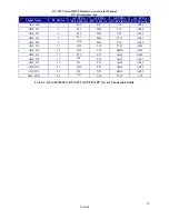
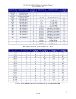
10.5.1
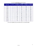
USB Interface for DP FPGA Interconnection Table


