
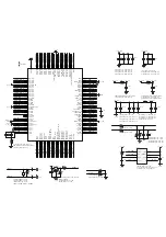
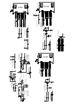


GND
FB1
FCM1005KF-121T06(120ohm-500mA)
GND
GND
3V3_STB
GND
CL8
0.1uF-0402-Y5V-+80%-20%-16V
CL9
0.1uF-0402-Y5V-+80%-20%-16V
1V8_DDR
RF4
100Kohm-0402-± 5%-1/16W
RESET_H
3V3_STB
RF3
1Kohm-0402-±5%-1/16W
QF1
SGM810-SXN3L
GND
XTALI
XTALO
CF2
33pF-0402-NPO-±5%-50V
CF1
33pF-0402-NPO-±5%-50V
GND
GND
R99
1Mohm-0402-±5%-1/16W
3V3_STB
CE#
1
SO
2
WP#
3
VSS
4
SI
5
SCK
6
HOLD#
7
VDD
8
UF1
GD25Q16BSIG
SPI_SCK
SPI_CSN
SPI_SDI
SPI_SDO
RF12
10Kohm-0402-± 5%-1/16W
#F_WP
GND
PWM/ADJ
BL_EN
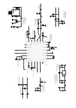
LVA0M
70
SOGIN1
22
BIN1P
21
GIN1M
24
GIN1P
23
CVBS0
28
CVBS1
27
AUL1
36
GIN0P
16
GP
IO
0/
G
PI
O
44
55
LV
ACKM
64
VDD
C
/D
VDD_
DDR_
C
M
D
54
VDD
IO_
CM
D
53
AVDD_MOD
5
RIN1P
25
HOTPLUG_C/D
80
LVA1P
67
LVB3P
71
DDCDB_
CL
11
2
DDCDB_
D
A
11
1
GIN0M
17
IRIN
93
CEC
92
TEST
91
DDCA_CK
90
DDCA_DA
89
LV
A
3M
62
LV
ACKP
63
LVA2P
65
LVA2M
66
DP_P0
97
LVB2P
74
LVB2M
75
LVB1P
76
LVB1M
77
LCK/LVB0P
78
PWM0
83
AVDD_MOD
73
DM_P0
96
HOTP
LU
G
_B
11
3
AVD
D_5
V
11
4
GND
_EF
US
E
11
5
RX0
P_
B
12
8
VI
FP
46
VI
FM
47
AUO
U
TR
0
44
IF
AG
C
45
XI
N
50
A
V
DD
3P
3_D
M
PL
L
49
XOU
T
51
RX1N_B
1
RX1P_B
2
RX2N_B
3
RX2P_B
4
RXCN_A
6
RXCP_A
7
RX0N_A
8
RX0P_A
9
RX1N_A
10
RX1P_A
11
RX2N_A
12
RX2P_A
13
HSYNC0
14
BIN0P
15
RIN0P
18
VSYNC0
19
AVDD3P3_ADC
20
VCOM
29
CVBS_OUT1
30
VDDC
31
AVDD_AU33
32
VAG
37
AUL0
34
AUR1
35
AUR4
40
AUO
U
TL
3
41
AVD
D
_M
OD
52
GP
IO
3/
G
PI
O
47
58
GP
IO
4/
G
PI
O
48
59
LV
A
3P
61
GP
IO
2/
G
PI
O
46
57
LVA0P
69
LVB3M
72
LVA1M
68
LDE/LVB0M
79
HOTPLUG_A
81
SPI_DO
84
SPI_DI
85
SPI_CZ
86
PWM1
82
VDD
IO_
DATA
10
5
DDCDC_
CL
10
6
DM_P1
98
VDD
C
/D
VDD_
DDR_
DAT
A
10
4
DP_P1
99
AVDD_MOD
100
DDCDA
_DA
10
9
INT/GPIO64
94
VDD
C
/A
VDDL_DV
I
11
6
RESET
95
MH
L_
D
ET
11
0
DDCDC_
D
A
10
7
DDCDA
_CL
10
8
E-
PA
D
12
9
VSYNC1
26
AUR0
33
AUO
U
TL
0
43
AUO
U
TR
3
42
GP
IO
1/
G
PI
O
45
56
SPI_CK
87
RXCN_
D
11
7
RXCP_
D
11
8
RX0
N
_D
11
9
RX0
P_
D
12
0
RX1
N
_D
12
1
RX2
N
_D
12
3
RX2
P_
D
12
4
RX1
P_
D
12
2
RXCP_
B
12
6
RX0
N
_B
12
7
RXCN_
B
12
5
VRM
38
AUL4
39
SAR1
102
SAR0
101
SA
R2
10
3
GP
IO
5/
G
PI
O
49
60
ARC
88
AVD
D
3P
3_
DADC
48
U1
MSD3393LU
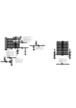
BL_EN
PWM/ADJ
CVBS1_OUT
M
H
L
_
CABL
E-
DET
HDM
I3
_
D
E
T
AM
P-
M
U
T
E
ARC_
DET
AU_VRM
IF
_
A
G
C
VI
FP
VI
FM
AU_VAG
+3_3V_AU
1.15V_STB
GIN1M
HD1_SOG
HD1_Pr
HD1_Y
HD1_Pb
VGA_RIN
VGA_GIN
VGA_BIN
GIN0M
VGA_HS
VGA_VS
AV_
L
IN
AV_
R
IN
AV_IN
VCOM
HDMI-ARC
HOTPLUG3'
HDM
I2
_
S
CL
HDM
I2
_
SDA
H
D
M
I2_RX
C_N
HDM
I2
_
R
X
C
_
P
H
D
M
I2_RX
0_N
H
D
M
I2_RX
0_P
HDMI2_RX1_N
HDMI2_RX1_P
HDMI2_RX2_N
HDMI2_RX2_P
HOTPLUG1'
HDM
I1
_
S
CL
HDM
I1
_
SDA
H
D
M
I1_RX
C_N
HDM
I1
_
R
X
C
_
P
H
D
M
I1_RX
0_N
H
D
M
I1_RX
0_P
H
D
M
I1_RX
1_N
H
D
M
I1_RX
1_P
HDM
I1
_
R
X
2
_
N
HDM
I1
_
R
X
2
_
P
HDM
I3
_
SCL
HDM
I3
_
SDA
HDMI3_RXC_N
HDMI3_RXC_P
HDMI3_RX0_N
HDMI3_RX0_P
HDMI3_RX1_N
HDMI3_RX1_P
HDMI3_RX2_N
HDMI3_RX2_P
HO
T
P
L
U
G
2
'
HDMI-CEC
UART-TX/DDC
UART-RX/DDC
LED_RED
REMOTE
RESET_H
KEY
SPI_CSN
SPI_SCK
SPI_SDI
SPI_SDO
3V3_STB
RXO2_N
RXO3_P
RXO3_N
RXO2_P
RXO0_N
RXO1_P
RXO1_N
RXO0_P
RXE3
_
P
RXE2_N
RXE1_P
RXE1_N
RXE0_N
RXE0_P
RXE2_P
RXE3
_
N
RXEC_
N
RXEC_
P
M_
S
C
L
M_
S
D
A
XTAL
I
XTAL
O
SPDI
F_
O
U
T
PO
W_
EN
PC_LIN
PC_RIN
AM
P-
L
O
'
AM
P-
RO
'
LI
N
E
_L_OU
T
LI
N
E
_R
_OU
T
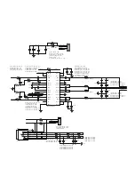
CL16
1uF-0402-X5R-± 20%-6.3V
GND
1.15V_STB
CD7
0.1uF-0402-Y5V-+80%-20%-16V
CD8
0.1uF-0402-Y5V-+80%-20%-16V
CD9
0.1uF-0402-Y5V-+80%-20%-16V
CD10
0.1uF-0402-Y5V-+80%-20%-16V
3V3_STB
C3
10uF-0603-X5R-± 20%-6.3V
C4
0.1uF-0402-Y5V-+80%-20%-16V
FB2
FCM1005KF-121T06(120ohm-500mA)
CL17
0.1uF-0402-Y5V-+80%-20%-16V
GND
3V3_STB
FB3
FCM1005KF-121T06(120ohm-500mA)
CL18
0.1uF-0402-Y5V-+80%-20%-16V
GND
+3_3V_AU
+3_3V_PLL
CL19
1uF-0402-X5R-± 20%-6.3V
CL10
0.1uF-0402-Y5V-+80%-20%-16V
CL12
0.1uF-0402-Y5V-+80%-20%-16V
CL13
0.1uF-0402-Y5V-+80%-20%-16V
CL14
0.1uF-0402-Y5V-+80%-20%-16V
FB4
FCM1005KF-121T06(120ohm-500mA)
+3_3V_ADC
CL20
1uF-0402-X5R-± 20%-6.3V
CL15
0.1uF-0402-Y5V-+80%-20%-16V
3V3_STB
3V3_STB
GND
3V3_STB
3V3_STB
+3_3V
_
A
D
C
+3_3V
_
P
L
L
1.
15V
_
S
T
B
1V
8_D
D
R
3V
3_S
T
B
GND
1.
15V
_
S
T
B
AVDD5
V_
M
H
L
1V
8_D
D
R
1
.1
5
V_
STB
GND
CF7
0.1uF-0402-Y5V-+80%-20%-16V
GND
C5
1000pF-0402-X7R-±10%-50V
C6
1000pF-0402-X7R-±10%-50V
GND
AMP-LO'
AMP-RO'
R5
200Kohm-0402-± 5%-1/16W
R6
200Kohm-0402-± 5%-1/16W
AMP-LO
AMP-RO
USB1_DM
USB1_DP
CVBS1_OUT
TEST
USB0_DM
USB0_DP
R1
4K7ohm-0402-± 5%-1/16W
R2
4K7ohm-0402-± 5%-1/16W
DVD_LIN
DVD_RIN
DVD_EN'
Y1
24MHz-±20PPM-20PF-HC-49S-SMD
CF17
NC/0.1uF-0402-Y5V-+80%-20%-16V
CF16
NC/0.1uF-0402-Y5V-+80%-20%-16V
GND
C14
0.1uF-0402-Y5V-+80%-20%-16V
GND
R3
0ohm-0402-± 5%-1/16W
R4
0ohm-0402-± 5%-1/16W
Summary of Contents for 40DR3505
Page 10: ...Service Manual Model No 2 2 External pictures four faces Front Side Up Side 9 40DR3505 ...
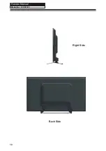
Page 11: ...Service Manual Model No Right Side Back Side 10 40DR3505 ...
Page 16: ...Service Manual Model No 15 40DR3505 ...
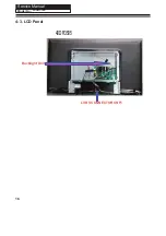
Page 17: ...Service Manual Model No 4 3 LCD Panel Backlight Unit LVDS CONNECTOR CNF1 16 40DR3505 40DR3505 ...
Page 18: ...Service Manual Model No 17 40DR3505 ...
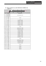
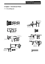
Page 31: ...Service Manual Model No 7 2 Wiring Connection Diagram 30 40DR3505 ...
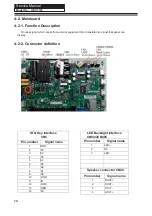
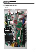
Page 37: ...Service Manual Model No 9 2 Mainboard IC Introduction Top view 36 1 2 3 4 5 6 7 8 40DR3505 ...
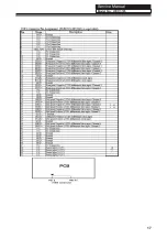
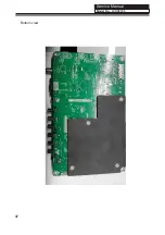
Page 38: ...Service Manual Model No Bottom view 37 40DR3505 ...