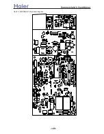

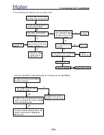
>a__WcU[S^ <[c >a`V[e[a`Wc
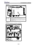
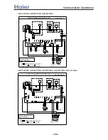
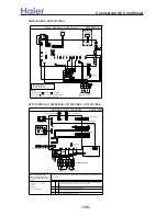
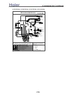
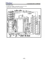
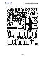
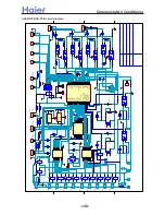
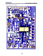
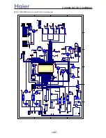
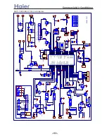
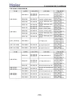
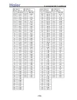
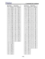
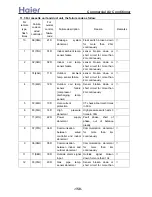
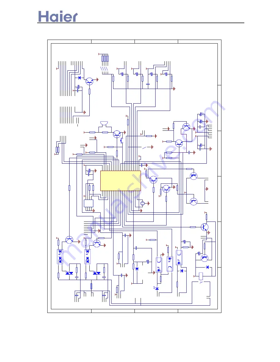
AF07~142XCBAA main control PCB circuit diagram:
P7
7
1
P7
6
2
P7
5
3
P7
4
4
P7
3
5
P7
2
6
P7
1
7
P7
0
8
P0
7
9
P0
6
10
P0
5
11
P0
4
12
P0
3
13
P0
2
14
P0
1
15
P0
0
16
TES
T
17
RE
SE
T
18
XIN
19
XOUT
20
VS
S
21
VAR
EF
22
P6
0
23
P6
1
24
P6
2
25
P6
3
26
P6
4
27
P6
5
28
P6
6
29
P6
7
30
P1
0
31
P1
1
32
P1
2
33
P1
3
34
P1
4
35
P1
5
36
P1
6
37
P1
7
38
P2
0
39
P2
1
40
P2
2
41
VC
C
42
IC
7
T
M
P
87P
H
4
6N
BU
Z
A1
1
A2
2
A3
3
A4
4
A5
5
A6
6
A7
7
Q1
16
Q2
15
Q3
14
Q4
13
Q5
12
Q6
11
Q7
10
VC
C
9
GN
D
8
IC
9
U
L
N
2
003A
Q1
9014
R3
1
5
.1
K
R4
5
1
0
K
R
4
4
10K
R5
2
1K
C9
4.7U
/50V
R2
9
20K
C7
4.7U
/50V
R
3
0
20K
C8
4.7U
/50V
R3
2
5
.1
K
C1
0
4.7U
/50V
R3
3
5
.1
K
VC
C
VC
C
VC
C
VC
C
VC
C
R4
1
10K
KEY
VC
C
R9
100
R1
3
220
IC
2
3021
C1
9
0.01U
/275V
R1
5
1K
R1
7
100
R1
4
220
C1
8
0.01U
/275V
R1
6
1K
C2
3
1.2U
/450V
C2
6
1.2U
/450V
Q2
9014
VC
C
VC
C
R1
2
5.1K
R3
6
5.1K
Q1
1
9014
R3
7
5.1K
D1 IN
4148
+12
VC
C
+12
12V
5
V
ZER
O
C2
100U
F
C1
104
VC
C
R4
2
100K
/2W
R5
1
20K
R1
0
1K
C2
4
104
VC
C
D3
IN
4148
R1
1
10K
C2
5
4.7U
/50V
R4
3
10K
VC
C
R5
0
1K
VC
C
C1
6
10U
F
C1
7
104
C1
2
100U
F
C1
1
104
R2
5
10K
R2
2
10K
VC
C
R2
3
10K
R2
4
10K
Q1
0
9013
Q9
9013
+12
Q4
9014
Q8
9014
Q7
9014
R6
10K
R4
560
R5
1K
R3
5.1K
VC
C
C2
0
103
R7
51K
VC
C
C2
2
103
R8
51K
IC
4
P5
2
1
8
7
6
5
4
3
2
1
IC
6
24L
C
0
1B
LE
D
4
VC
C
VC
C
VC
C
R1
8
10K
R
1
9
10K
JK
1
12V
(220V
)
+12
D2
IN
4148
R1
2
K
R2
1
10K
R2
0
10K
R3
4
5.1K
R3
5
5.1K
+12
+12
A0
A1
A2
VS
S
S
DA
SCL
WP
VC
C
Q3
2S
B
1240
R2
51K
+12
C1
3
103
1
CN4
1
CN3
B2B-
XH
C3
47U
/16V
C4
220U
F
C5
104
VC
C
4*
10K
R
46-
R
4
9
R3
9
10K
Q6
2S
B
1240
Q5
2S
B
1
240
+12
R2
8
2K
R2
7
2
K
VC
C
1
2
3
CN
2
8
1
2
3
CN
7
ST
R
1
D
2
CL
K
3
OE
15
Q1
4
Q2
5
Q3
6
Q4
7
Q5
14
Q6
13
Q7
12
Q8
11
QS
9
QS
10
IC
8
B
U
4094
1
2
CN
2
3
IC
1
3
0
2
1
1
2
3
4
5
6
7
8
CN
2
7
1
2
3
CN
5
1
2
3
CN
6
TR
2
TR
1
1
2
3
4
5
6
7
8
CN
1
2
+12
1
2
3
4
5
CN
2
1
1
2
CN
8
1
2
CN
9
A
1
2
CN
9
1
2
CN
1
0
1
2
CN
1
1
1
2
CN
1
3
1
2
CN
1
6
1
2
CN
1
7
1
2
CN
2
2
1
2
CN
2
4
1
2
CN
2
6
Vi
n
1
GND
2
Vou
t
3
IC
3
T
600D
1
2
3
OS
C
8M
1
2
3
4
5
6
7
CN
2
0
VC
C
JP
1
JP
2
JP
3
JP
4
SW
1
2
CN
1
1
2
CN
2
FU
S
E
C2
1
103
L
N
GN
D
R
4
0
10K
VC
C
R5
4
100
R5
3
10K
+12
1
2
3
4
CN
1
5
Q1
2
9014
IC
1
0
P
521
C2
7
4.7U
/50V
VC
C
D4
IN
4148
IC
5
P
5
2
1
C4
10U
F
C2
8
104
-147-
Summary of Contents for AB072XCBAA
Page 21: ... a__WcU S c a V e a Wc AU84NXTBAA 66 33 1 23 4 43 33 61 2 3 160 2 15 3 52 21 ...
Page 138: ... a__WcU S c a V e a Wc AU282XHBAA AU422XIBAA PCB printed diagram 138 ...
Page 141: ... a__WcU S c a V e a Wc AU84NXTBAA PCB printed diagram 141 ...
Page 144: ... a__WcU S c a V e a Wc AB AE AD units PCB printed diagram 144 ...
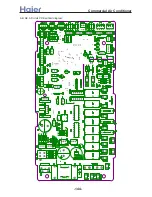
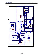
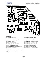
Page 149: ... a__WcU S c a V e a Wc AF07 142XCBAA PCB printed diagram 149 ...
Page 180: ...MEMO Commercial Air Conditioner ...


