background image

33 

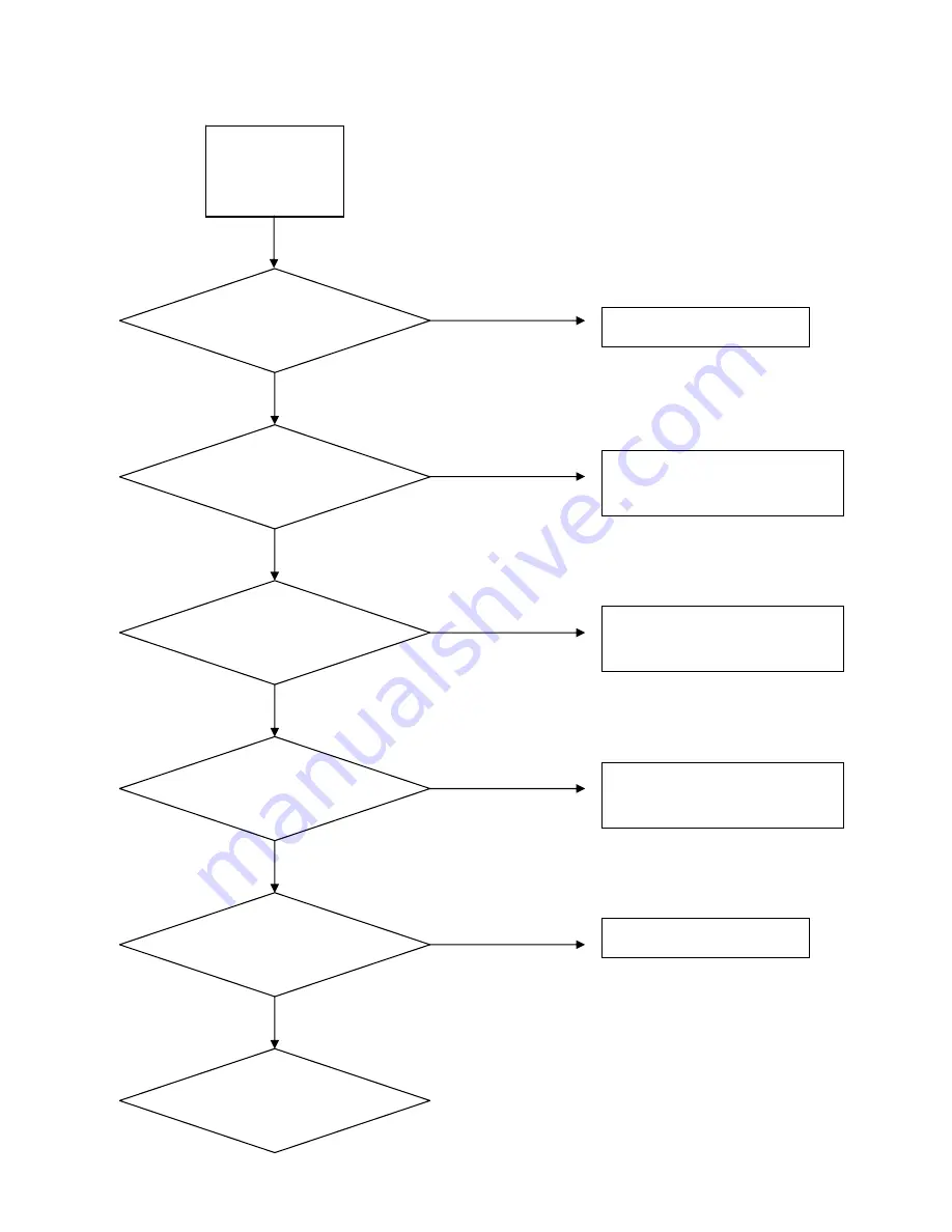
9.3 Main board failure check 

State: No picture 


Fail 


                            Pass 


 Fail 


                            Pass         


 Fail 


                            Pass                                                     


 Fail 


                            Pass 


  Fail 


                            Pass 


No Sound 

(All Mode) 

Check the input   

        Source 

Change Source input 

Check the input/output 

Of    IC U13 of Main B/D 

Re-soldering or change 

IC U13 

Check the input/output 

Of IC U55 of Main B/D 

Re-soldering or change 

IC U55 

Check the input/output 

Of IC U2 of Main B/D 

Re-soldering or change 

IC U2 

Check the Speaker 

Change the Speaker 

Check the Sperker 

wire 

Summary of Contents for DX-LTDVD19-09

Page 1: ...1 DX LTDVD19 09 2008 Haier Electronic Company Limited All rights reserved Unauthorized copying and distribution is a violation of law ...

Page 2: ...PECIFICATIONS 3 2 WAINING 4 3 LOCATION OF CONTROLS AND COMPONENTS 6 3 1 Board Location 6 3 2 Main Board AV Board 7 3 3 Power Board 9 3 4 LCD Panel 10 4 External Equipment Connections 11 5 OPERATION INSTRUCTIONS 15 5 1 Front Panel Controls 15 5 2 Back Panel Controls 16 5 3 Universal Remote Controller 17 6 DISASSEMBLY INSTRUCTIONS 18 6 1 Whole Machine 18 6 2 Support Stand Assembly 19 6 3 Back Cabine...

Page 3: ... output power Built in W 2 3W Audio output power outer W No Total power input W 80W Voltage range V AC120V Power frequency Hz 60Hz Time of sleep timer MINS 5 10 15 30 60 90 120 180 240 Net weight KG 5 Gross weight KG 6 35 Net dimension MM 462 179 5 388 5 Packaged dimension MM 522 203 438 Notes 1 NTSC Standards Developed by National TV Standards Committee 2 M standard each channel bandwidth is 6 MH...

Page 4: ...al installation This equipment generates use and can radiate radio frequency energy and if not installed and used in accordance with the instructions may cause harmful interference to radio communications However there is no guarantee that interference with not occur in a particular installation If this equipment does cause harmful interference to radio or television reception which can be determi...

Page 5: ... local power company 9 Do not defeat the safety purpose of the polarized or grounding type plug A polarized plug has two blades with one wider than the other A grounding type plug has two blades and a third grounding prong The wide blade or the third prong are provided for your safety If the provided plug does not fit into your outlet consult an electrician for replacement of the obsolete outlet T...

Page 6: ...xtensive work by a qualified technician to restore the unit to its normal operation e If the unit has been dropped or damaged in any way f When the unit exhibits a distinct change in performance this indicates a need for service 15 Heat The product should be situated away heat source such as radiators heat registers stoves or other products Including amplifiers that product heat 16 Overloading Do ...

Page 7: ... panel can display 3 2 2 Connector definition Main board connector Power connectors CN3 CN5 Notes CN3 Pin 3 Backlight on off The system can turn on or turn off the backlight of TFT LCD Panel through the power supply unit path CN3 CN5 Pin number Signal name Pin number Signal name 1 12V 1 12V 2 12V 2 GND 3 BL 3 GND 4 DIM 4 5V 5 GND 5 STB 6 GND 7 SW ...

Page 8: ... to control the strength of TFT LCD Panel s backlight through this connector Keypad and remote connector CN2 Speaker connector CN1 DVD VIDEO Connector CN6 Pin number Signal name Description 1 GPIO GPIO 2 PB_IN PB1 IN 3 Y_IN Y1_IN 4 GND GND 5 PR_IN PR1 IN 6 GND GND 7 IR DVD IR DVD AUDIO Connector P1 Pin number Signal name Description 1 LI YPBPR1L_IN 2 RI YPBPR1R_IN 3 GND GND ...

Page 9: ...5380C U13 AND FLASH U17 U0TX 3V3SB U0RX J3 4x1 W HOUSING DIP4 W H P2 0 1 2 3 4 3 3 Power Board 3 3 1 Function Description Supply power for Main board Panel 3 3 2Connectordefinition INPUT CONNECTOR CN6 CN10 Signal name 1 N 2 GND 3 GND 4 DIM 5 EN 6 12V 7 12V ...

Page 10: ...11 A2N LVDS EVEN 2 Signal 12 A2P LVDS EVEN 2 Signal 13 14 GND Ground 15 CK1N LVDS EVEN Clock Signal 16 CK1P LVDS EVEN Clock Signal 17 A3N LVDS EVEN 3 Signal 18 A3P LVDS EVEN 3 Signal 19 A4N LVDS ODD 0 Signal 20 A4P LVDS ODD 0 Signal 21 A5N LVDS ODD 1 Signal 22 A5P LVDS ODD 1 Signal 23 A6N LVDS ODD 2 Signal 24 A6P LVDS ODD 2 Signal 25 26 GND Ground 27 CK2N LVDS ODD Clock Signal 28 CK2P LVDS ODD Clo...

Page 11: ...8 LVDS EVEN LVDS EVEN Signal 19 24 27 28 29 30 LVDS ODD LVDS ODD Signal 4 External Equipment Connections Accessories Remote Control User GUIDE Battery Antenna Connection 1 Connect one end of a coaxial cable not included to the ANT IN jack on the back of your TV DVD combo then connect the other end of the cable into the antenna or cable TV wall outlet ...

Page 12: ...t two TVs install a two way splitter Choose Your Connection There are several ways to connect your television depending on the components you want to connect and the quality of the signal you want to achieve The following are examples of some different ways to connect your TV with different input sources Choose the connection which is best for you ...

Page 13: ...13 VCR connection ...

Page 14: ...14 External Equipment Connections ...

Page 15: ...15 5 OPERATION INSTRUCTIONS Basal information 5 1 Front panel controls ...

Page 16: ...16 5 2 Back panel controls ...

Page 17: ...17 5 3 Universal Remote Controller ...

Page 18: ...t Assembly Base Assembly Main board Assembly Remote Control Board Assembly Control Board Assembly Assembly Material Subassembly Romote Contral Per setting Assembly 1 2 3 1 3 2 3 3 3 4 3 5 3 6 3 7 Components List NO Name Description Parts number 1 DX LTDVD19 09 2 Packaging 3 TV Set 3 1 Base Borad 3 2 Back Cabinet 3 3 Control PCB ...

Page 19: ...0100M 3 7 DVD DC11Z0E0100D 6 2 Support Stand Assembly Assembly Spare parts number Locatio n No Spare Parts Name in English Specificatio n Qty Support Stand Assembly 1 Support Stand Subassembly 1 Base Board 1 Rotational Axis 1 Rubber 5 Bolt Support Stand Assembly 4 Support Stand Assembly Bolt GB818 85 M4X16 4 ...

Page 20: ...rd bracket 1 Power Board bracket 2 Terminal Board 1 LCD panel bracket 2 Small cover board 1 Bolster 1 Screw 2 Speaker Y47 418 5W 4Ω 2 DVD shield metal 1 DVD Button Label Sponge Strip 0 17 Bolt 2 Bolt GB818 85 M3 4 4 Bolt SJ2824 87 ST4X12F 6 Bolt SJ2824 87 ST4 16F 1 Bolt SJ2824 87 ST3X8F 8 Terminal Lable black 1 Bolt SJ2824 87 ST3 8F 8 Bolt SJ2824 87 ST3 8F 8 Bolt SJ2824 87 ST3 8F 3 Back Cabinet As...

Page 21: ...cification Qty Front Cabinet Assembly 1 Front Cabinet Subassembly 1 Plastic Front Cabinet 1 Transparent Window silk screen DYNEX 1 Plastic board 1 Bolt SJ2824 87 ST3X10F 2 LCD Pannel T190PW01 1 LOGO Front Cabinet Assembly Bolt SJ2824 87 ST3 10F 2 6 5 Miscellaneous Material Assembly 6 5 1 Location Photo ...

Page 22: ...ly 1 LVDS Connection Wire 1 Speaker Connection Wire 1 Connection Wire 1 Power Cord 1 Power Mainboard Inverter Connective Wire 1 Power Supply Board 1 Left Gasket 1 Right Gasket 1 Magnetic Loop 2 Magnetic Loop 2 ROHS DVD 1 ROHS DVD Signal Wire 1 ROHS DVD Power wire 1 Metal clip 3 Screw 3 Miscellaneous Material Assembly Damper Foam 3 ...

Page 23: ......

Page 24: ......

Page 25: ... 2sec input 8893 Finished these operations system will be into the factory mode menu IF want to exit this factory menu please press the botton Exit in the remoter 7 1 Version S N Panel Resoution Version The first line is the model Name and the second line is current software version ...

Page 26: ... be used in the VGA and Component model When we found the color in the two models was abnormal Then we can use the function to adjust it automatically 7 2 2 Color Temperature The function could adjust the Color Temperature used when debugging 7 3 Audio ...

Page 27: ...e RF atv line AV S Video YPbPr VGA Compression Factor Compression state Downmix output model MTS System used when debugging The parameters only used when debugging no need to be modified 7 4 Channel Range Scan The function could make it to search the channels by differentiation the analog and digital channels ...

Page 28: ... Single RF Scan Search channels in the frequency scope set in advance Factory Scan According to ANTENNA ANALOG ANTENNA DIGITAL CABLE ANALOG CABLE DIGITAL to search channels used only in project debugging ...

Page 29: ...27 Tuner Diagnostic Project debugging setting used to inspect the audio function 7 5Gamma Gamma Bright GAMMA0 8 Middle default settings in the program Dark GAMMA1 2 ...

Page 30: ...djust the backlight 7 7 Function Burning Mode Turn it ON to enter the aging model This is for factory run in testing The screen would display red green blue and black screen repeatedly Each color screen could be exam at that time ...

Page 31: ...29 Clean Storage The function could make the model turn back to the factory default setting Remark The date of the chart only is a example please don t adjust the factory mode base on it ...

Page 32: ...30 8 WIRING CONNECTION DIAGRAM ...

Page 33: ...n some channel Verify if correct channel is selected Adjust the antenna Make adjustments by Fine Tune and MANUAL Scan No color for some channel program black and white Verify if the same problem exists in other channels check out of picture and sound system Refer to relative instructions in the Manual for color adjust Spots with some or all pictures Verify if the antennal is correctly connected Ve...

Page 34: ... failure check State No power First check cables which connect with PSU then check as follows 1 Check PSB input voltage AC input voltage 120V connector CN7 2 Check PSB output voltage orderly voltage 12V 12V connector CN3 P6 P7 ...

Page 35: ...ck the input Source Change Source input Check the input output Of IC U13 of Main B D Re soldering or change IC U13 Check the input output Of IC U55 of Main B D Re soldering or change IC U55 Check the input output Of IC U2 of Main B D Re soldering or change IC U2 Check the Speaker Change the Speaker Check the Sperker wire ...

Page 36: ...el Check the backlight B D Change the backlight B D Check the input output of jack CN3 of Main B D Re soldering or change IC UA1 and RNA1 17 Check the input output of Jack CN4 of Main B D Re soldering or change IC U13 Change the panel Change the Panel wire Check the Panel wire ...

Page 37: ...P Sunken TCP lead cracking ACF bonding short Awful environment and something electric enter into LCD Mis align between TCP and Panel Panel failure TCP failure Failure Mode Part Name Description Phenomena Failure cause Dot Defect Bright dot dark dot in pannel Incoming Inspection Standard Polarizer Bubble Bladder in Polarizer Bladder between Polarizer and top glass Polarizer Scratch Polarizer Scratc...

Page 38: ...mbalance Abnormal Color Only color abormal Capacitance improper bring crosstalk inside LCD pannel Circuit Abnormal Color Only color abnormal 1 Chip lose action 2 IC short or jointion bad 3 Pannel and vsc connect bad Failure Mode Part Name Description Phenomena Failure cause Mechanlcal Nolse When turn panel appear cacophony Caused by Mechanica noise of backlight unit Ripple Connectric circle Causee...

Page 39: ... in B L unit is uneven Mechanlcal or B L Mount hole Lack screw or screw damage Lack screw Screw damage 10 MAINTENANCE To remove dirt or dust wipe the cabinet with a soft dry lint free cloth Please be sure not to use a wet cloth Cleaning the Screen Early malfunctions can be prevented Careful and regular cleaning can extend the amount of time you will have your new TV Be sure to turn the power off a...

Page 40: ... dry before you turn on your TV Cleaning the Cabinet Extended Absence If you expect to leave your TV dormant for a long time such as a vacation it s a good idea to unplug the power cord to protect against possible damage from lightning or power surges 11 CIRCUIT DIAGRAM ...

Page 41: ...10 12V GPIO_10 GPIO_3 PB1_IN PR1_IN OIRI GPIO_11 Y1_IN DVD_IR GPIO_11 Y1_IN PB1_IN PR1_IN SW_POWER 5VSB OIRI 3V3SB DVD_IR OPWRSB OPWRSB OIRI 7 GND 2 3 4 5 6 7 8 9 10 11 12 13 14 3V3SB 2 4 7 8 9 OPCTRL3 4 5VSB 2 9 11 ADIN2 4 12V 2 3 8 9 14 ADIN1 4 5V 2 3 8 9 14 BL_ON OFF 9 DIMMING 9 GPIO_3 4 GPIO_10 4 GPIO_11 4 PB1_IN 10 PR1_IN 10 Y1_IN 10 OPWRSB 4 3V3SB DC 12V DC 12V 5VSB 12V DC 12V 3V3SB 5V 5V_DV...

Page 42: ...4 5V 3V3SB 5VSB DV33 12V DV10 DDRV VTT 5V DDRV DDRV AV33 CE593 470uF 16v R956 110 R29 NC R43 1 5K R32 NC CB12 0 1uF L134 NC CB37 0 1uF R7 2K R10 110 U4 IC LP2996 DDR Termination SOP 8 1 2 3 4 5 6 7 8 GND SD VSENSE VREF VDDQ AVIN PVIN VTT R519 100K R1 110 CB64 0 1uF U11 LT1084 TO 252 3 3 1 2 IN ADJ GND OUT R11 180 C301 NS 100nF CE33 470uF 6 3v R5 1K CB33 0 1uF CB8 0 1uF CE17 100uF 10v R6 4 7K C302 ...

Page 43: ... 12V OPWM2 GND 1 2 4 5 6 7 8 9 10 11 12 13 14 5V 1 2 8 9 14 AV33 2 5 8 9 13 AV12 5 8 10 5V_TUNER 5 12 AV25 5 12 12V 1 2 8 9 14 OPWM2 4 7 5V AV33 AV25 5V 5V_TUNER AV12 AV25 12V R12 110 U10 AZ1117 adj 1 2 3 ADJ GND OUT IN CB32 0 1uF CB228 0 1uF R14 180 CB197 0 1uF R19 0 C575 1uF U7 AZ1117 adj 1 2 3 ADJ GND OUT IN CE19 470uF 6 3v CB229 0 1uF CE22 100uF 10v C573 1uF CE30 100uF 10v CE28 100uF 6 3v L146...

Page 44: ...DIN1 1 ADIN2 1 OPCTRL3 1 GPIO_3 1 GPIO_10 1 GPIO_11 1 DV33 3V3SB DV33 3V3SB 3V3SB 3V3SB DV33 DV33 DV33 3V3SB H2 HOLE GND 2 3 4 5 9 8 7 6 1 2 3 4 5 9 8 7 6 1 R28 10K R52 NC TP34 C21 5pF R22 47K R198 10K R40 4 7K C22 1uF R27 1 H3 HOLE GND 2 3 4 5 9 8 7 6 1 2 3 4 5 9 8 7 6 1 FB17 FB Q1 2N3904 1 3 2 R199 NC R25 390 TP36 CB70 0 1uF R21 220 Y1 60MHz R30 33 R35 NC H4 HOLE GND 2 3 4 5 9 8 7 6 1 2 3 4 5 9 ...

Page 45: ...ATA SIFP RF_AGC SIFN TUNER_CLK AF AVDD25_SADC T1 TUNER_ALPS TH1 TH2 TH3 TH4 1 2 3 4 5 6 7 8 11 12 13 14 15 16 17 18 19 20 21 GND1 GND2 GND3 GND4 NC or OOB B1_ 5V GND or SIF O P GND or CVBS RF_AGC Mon NC or AFT NC or IF_AGC Mon NC or B2_Ana_ 5V TU_ 32V GND GND SCL SDA AS B_IF O P D_IF_AGC NC D_IF_O P_1 D_IF_O P_2 CB450 NS 100pF C42 0 01uF C0603 SMD C41 1uF C70 10nF CE38 100uF 6 3v R34 5 1K 1 FB34 F...

Page 46: ...2 7 GND 1 2 3 4 5 7 8 9 10 11 12 13 14 MEM_VREF 2 VTT 2 VTT DDRV VTT DDRV DDRV VTT VTT RA6 75 RA10 NS 75 CA23 4 7uF 10V CA3 0 1uF 0402 RNA1 47x4 0402 1 2 3 4 5 6 7 8 RNA10 47x4 0402 RN0402 SMD 1 2 3 4 5 6 7 8 RNA17 75x4 1 2 3 4 5 6 7 8 CA20 0 1uF CA5 0 1uF 0402 RA8 75 RNA4 47x4 0402 1 2 3 4 5 6 7 8 RA7 75 RNA6 47x4 0402 1 2 3 4 5 6 7 8 RA14 100 CA27 0 1uF UA1 16M x 16 DDR TSOP 66 1 2 3 4 5 6 7 8 9...

Page 47: ... U13J MT5380 SMD LQFP 252 251 250 249 95 94 253 1 256 255 254 93 POCE0_ POOE_ PDD0 PDD1 U0RX U0TX JTMS JTRST_ JTCK JTDO JTDI OIRI R1209 0 R54 10K R45 4 7K R1257 NS 4 7K R61 4 7K U17 M25P16 NS 1 2 3 4 5 6 7 8 S_ Q W_ VPP VSS D C HOLD_ VCC CB452 0 1uF R1227 NS 4 7K CB52 0 1uF C0402 SMD RN5 10K X4 1 2 3 4 5 6 7 8 R197 NS 10K CA36 4 7uF 10V CA37 0 1uF C0402 SMD CB53 0 1uF C0603 SMD CA39 0 1uF C0603 SM...

Page 48: ...WR0 HDMI_PLUGPWR0 5V AV12 12V 12V 3V3SB 12VAMP 12V 12V C17 4 7uF 10v U23 EEPROM 24C02 1 2 3 4 5 6 7 8 NC NC NC GND SDA SCL WP VCC CB146 0 1uF C0603 SMD CE8 470uF 16v R97 1K R33 1K R94 20K DN2 PESD1206Q 140 PESD1206Q 140 SMD 1 2 3 4 5 6 7 8 C655 10uF 10v C0805 SMD R96 47K R625 4 7K L142 FB U2 TPA1517 TDA1517P 1 2 3 4 5 6 7 8 9 10 11 12 13 14 15 16 17 18 19 20 IN1 SGND SVRR OUT1 GND OUT2 VPP MUTE IN...

Page 49: ...14 DV33 2 4 7 14 DIMMING 1 BL_ON OFF 1 5V_LVDS 12V AV33 AV33 5VSB 3V3SB DV33 5V 5V 5V 12V 12V 5V_LVDS CB218 0 1uF TP45 C654 100nF C0603 SMD CB155 0 1uF C0603 SMD CB216 0 1uF TP46 CN4 15x2 DIP 15X2P P2 0 2 4 6 8 10 12 14 16 18 20 22 24 26 28 30 1 3 5 7 9 11 13 15 17 19 21 23 25 27 29 JP10 FB 1206 CB455 1uF R123 100K D164 SCHOTTKY DIODE B340A D SMA SMD L132 FB CE72 470uF 16v R1789 4 3K R0603 SMD R40...

Page 50: ...AV12 AV12 AV12 L140 80 100MHZ R1200 68 C659 10uF 10v C0805 SMD R1641 68 TP47 L82 80 100MHZ C351 10nF C115 1uF D105 NS EZJZ0V800AA ESD0603 SMD 1 2 C349 4 7nF C592 4 7nF R1635 100 R1639 100 R1184 68 C363 10nF R1640 75 C353 15pF R1636 68 D157 NS EZJZ0V800AA 1 2 R153 20K D160 NS EZJZ0V800AA ESD0603 SMD 1 2 R1203 75 D156 NS EZJZ0V800AA 1 2 C357 10nF R1189 100 C116 1uF CB160 0 1uF C0603 SMD C600 10nF C5...

Page 51: ...GPWR VGA_PLUGPWR 5VSB 5VSB C139 10nF D29 1N4148 FB67 80 100MHz R164 2K D27 NS EZJZ0V800AA 1 2 D32 NS EZJZ0V800AA 1 2 C661 10uF 10v C0805 SMD R180 100 R101 1K R0603 SMD C145 NS 0 1uF C134 5pF R170 2K R24 10K FB68 80 100MHz C135 10nF D31 NS EZJZ0V800AA 1 2 R160 0 R169 68 R181 0 R171 75 R182 10K R161 0 C137 5pF FB69 80 100MHz QF6 2N7002LT1 SOT23 SMD 1 3 2 R100 1K C136 10nF D23 NS EZJZ0V800AA 1 2 C141...

Page 52: ...43 FB R1213 NS 75 R190 20K C535 47nF Q4 2SD2653K NC 1 3 2 C663 10uF 10v C0805 SMD R1591 47 L33 0 C534 47nF L35 NS 330nH R1587 100 CB135 0 1uF R1594 27 C152 4 7uF 10V R81 10K NC R1592 100 L34 0 C459 47pF TP51 R1525 47 R79 100 D147 NS EZJZ0V800AA 1 2 C111 NS 43pF R1560 100 C567 10nF CB163 0 1uF C0603 SMD CE47 470uF 16V NC CB162 0 1uF C0603 SMD C536 47pF R1216 0 C112 NS 24pF R1562 47 D146 NS EZJZ0V80...

Page 53: ... 8 9 10 11 12 14 AIN0_R 12 AIN1_L 10 AIN1_R 10 AIN2_L 11 AIN0_L 12 AIN2_R 11 AR1 14 AL1 14 5V 1 2 3 8 9 14 MUTE 8 14 AV33 2 3 5 8 9 ASPDIF 10 12V 1 2 3 8 9 14 OFF_MUTE 14 AOLRCK 7 AOBCK 7 GPIO_ 4 11 1 4 8 9 14 OSCL0 4 OSDA0 4 OPCTRL1 4 11 CEC 4 8 3V3SB 1 2 4 7 8 9 AR2 14 AL2 14 HPDET 14 AIN3_L 10 AIN3_R 10 AV33 AV33 AV33 AV33 AV33 CB171 0 1uF C0603 SMD U13G MT5380 SMD LQFP 179 178 177 176 175 174 ...

Page 54: ...20pF NC R1758 NS 10K R1713 33K NC CE25 330uF 16V CN7 AV_OUT 6PX2 0 3 4 5 1 2 6 GND AOUTL GND AOUTR GND CVBSO FB70 FB CE631 22uF 10v R1725 NS 10K R1757 NS 10K R1755 5 1K R1783 3 9k D16 NS 1N4148 R1753 33K R1719 10K NC R1778 3 9k FB71 FB R1616 1K C668 10uF 10v C0805 SMD R298 5 1K R1721 10K NC R1718 NS 10K U55A NJM4558 OPA 3 2 1 8 4 C670 10uF 10v C0805 SMD R1717 NS 10K D15 1N4148 C666 10uF 10v NC C08...

Page 55: ...39 Sincere Forever ...

Reviews: