


A
A
A
A
AVDD33_H
AV33
OSDA1
OSCL1
RX0_CB
RX0_C
RX0_1B
RX0_1
RX0_2B
RX0_2
RX0_0B
RX0_0
OPWR0_5V
AVDD33_H
+12V
CEC
AVDD12_CVCC
AVDD12_CVCC
AV12
GPIO_[5..11]
+3V3SB
HDMIDDCSDA_0
OSDA1
HDMIDDCSCL_0
OSCL1
GND
HDMIDDCSCL_0
RX5V2_DDC_SCL
RX5V2_DDC_SDA
HD
HD
HDMI1_RX1-
HDMI1_RXC-
HDMIDDCSDA_0
CEC_H
POW0
POW2
RX5
V
2
_
DDC_
SDA
RX5
V
2
_
DDC_
SCL
HDM
I2
_
RXC-
HDM
I2
_
RXC+
H
D
MI2_R
X
0-
H
D
MI2_R
X
0+
AV33_HDMI
H
D
MI2_R
X
1-
CEC_H
H
D
MI2_R
X
1+
H
D
MI2_R
X
2-
H
D
MI2_R
X
2+
S2/SCL_CTL
OSCL0
RX5V1_DDC_SDA
RX5V1_DDC_SCL
RX2_HOTPLUG#
S3/I1C_ADDR
GPIO_6
HPD2
RX1_HOTPLUG#
OSDA0
HDMI1_RX0-
POW2
HPD1
RX1_HOTPLUG#
OSCL1
HD
OSDA0
HD
HD
RX5V1_DDC_SDA
RX5V2_DDC_SDA
HDMI2_RX2-
HD
HDMI1_RX2-
HD
HDMI1_RX1-
RX2_HOTPLUG#
HDMI2_RX1-
OSCL0
RX5V2_DDC_SCL
HDMI2_RXC-
HD
I2_RS
T
HDMI1_RX0-
RX5V1_DDC_SCL
HD
S1/SDA_CTL
HD
HDMI2_RX0-
HD
HD
HDMI1_RX0-
HDMI1_RX1-
HD
HDMI1_RX2-
HD
HDMI1_RXC-
RX5V1_DDC_SCL
RX5V1_DDC_SDA
REXT
SCL_SINK
SDA_SINK
RX0_2B
HPD_SINK1
RX0_CB
RX0_2
RX0_1B
RX0_1
RX0_C
RX0_0B
RX0_0
HDMI1_RXC-
GPIO_7
HDMI1_RX2-
HD
+5VSB
OP
W
R
0_5V
CEXT
PC1
POW0
HD
HD
HDMI2_RX2-
HD
HDMI2_RX1-
HDMI2_RXC-
HD
HDMI2_RX0-
HD
OSDA1
HDMI1_5VIN
HDMI1_5VIN
HDMIDDCWP0
HDMI2_5VIN
CEC_H
HDMI2_5VIN
CEC
AV33_HDMI
HDMI3_RXC-
HD
CEC_H
HDMI3_RX0-
HD
HDMI3_RX1-
HD
HDMI3_RX2-
HD
RX3_HOTPLUG#
HDMI3_5VIN
RX5V3_DDC_SDA
RX5V3_DDC_SCL
HDM
I3
_
R
X2
-
HDM
I3
_
R
X1
+
HDM
I3
_
R
X2
+
HDM
I3
_
R
X1
-
HDM
I3
_
R
X0
-
HDM
I3
_
RXC+
HDM
I3
_
RXC-
HDM
I3
_
R
X0
+
HPD3
PO
W1
HDMI3_5VIN
HDM
ISDA_
1
RX5V3_DDC_SDA
RX3_HOTPLUG#
HDM
ISCL
_
1
RX5V3_DDC_SCL
RX5V3_DDC_SDA
RX5V3_DDC_SCL
HDMI3_5VIN
RX0_2B
AV33_HDMI
RX0_1
RX0_1B
HDM
I2
_
RXC-
HDM
I2
_
R
X1
+
RX0_C
RX0_CB
SCL_SINK
SDA_SINK
GND
RX0_0
RX0_0B
HPD_SINK1
HDM
I2
_
RXC+
HPD3
HDMI1_RX2-
HD
POW0
HPD1
RX5V1_DDC_SDA
HDM
ISCL
_
1
HDM
ISDA_
1
A
V
33_H
D
M
I
HDM
I2
_
R
X2
-
RX5V1_DDC_SCL
HDMI1_RXC-
HPD2
HD
POW2
HDMI1_RX0-
HD
GND
HDMI1_RX1-
HD
AV33_HDMI
HDM
I3
_
RXC+
HDM
I3
_
R
X0
-
PO
W1
HDM
I3
_
RXC-
HDM
I2
_
R
X2
+
GND
HDM
I3
_
R
X1
+
HDM
I3
_
R
X1
-
HDM
I3
_
R
X2
-
CEXT
HDM
I3
_
R
X2
+
A
V
33_H
D
M
I
HDM
I3
_
R
X0
+
S1/SDA_CTL
REXT
OP
W
R
0_5V
HDM
I2
_
R
X0
-
PC1
HDM
I2
_
R
X0
+
S2/SCL_CTL
RX5
V
2
_
DDC_
SDA
GND
S3/I1C_ADDR
RX0_2
RX5
V
2
_
DDC_
SCL
I2_R
S
T
HDM
I2
_
R
X1
-
AV33
AV12
+5VSB
AV33
AV33_HDMI
+5VSB
+3V3SB
AV33_HDMI
AV33_HDMI
AV33_HDMI
AV33_HDMI
AV33_HDMI
AV33_HDMI
+3V3SB
+5VSB
+5VSB
OSDA1
4
OSCL1
4
GND
1,2,3,4,5,6,7,9,10,11,12,13,14
AV33
2,3,5,9,13
+12V
1,2,5,9,13,14
CEC
4
AV12
3,5,10
GPIO_[5..11]
1,4,9,13
+3V3SB
1,2,4,7,9
OSDA0
4
OSCL0
4
+5VSB
1,2,9,11
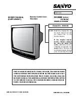
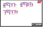
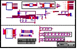
Title
Size
Document Number
Rev
Date:
Sheet
of
Drawn
MT5380P1-V2
V1
Custom
8
15
Tuesday, December 09, 2008
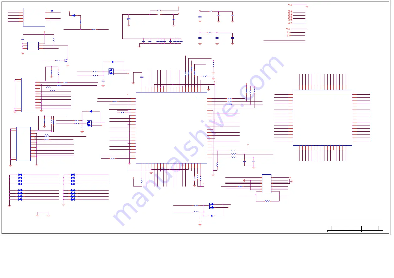
HDMI/SPEAKER
NUSTC_5380P1_V2
Title
Size
Document Number
Rev
Date:
Sheet
of
Drawn
MT5380P1-V2
V1
Custom
8
15
Tuesday, December 09, 2008
HDMI/SPEAKER
NUSTC_5380P1_V2
Title
Size
Document Number
Rev
Date:
Sheet
of
Drawn
MT5380P1-V2
V1
Custom
8
15
Tuesday, December 09, 2008
HDMI/SPEAKER
NUSTC_5380P1_V2
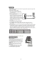
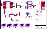
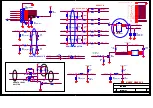
HDMI2 INPUT
HDMI1 INPUT
C17
4.7uF
C17
4.7uF
R2090
100
R0603/SMD
R2090
100
R0603/SMD
CB146
0.1uF
CB146
0.1uF
D207
D207
1
2
D217
BAV70
D217
BAV70
1
2
3
R103
4.7K
R0603/SMD
R103
4.7K
R0603/SMD
R2046
68R
R2046
68R
C4
1uF
C0402/SMD
C4
1uF
C0402/SMD
R2122
37K
R2122
37K
CB1008
2.2uF/10v
C0805/SMD
CB1008
2.2uF/10v
C0805/SMD
FB79
FB
BEAD/SMD/0603
FB79
FB
BEAD/SMD/0603
R2126
47K
R2126
47K
R2100
47K
R0603/SMD
R2100
47K
R0603/SMD
R1605
27K
R0603/SMD
R1605
27K
R0603/SMD
P5
HDMI/HAIER
HDMI/SMD/CON/A
P5
HDMI/HAIER
HDMI/SMD/CON/A
SHELL1
20
SHELL2
21
D2+
1
D2 Shield
2
D2-
3
D1+
4
D1 Shield
5
D1-
6
D0+
7
D0 Shield
8
D0-
9
CK+
10
CK Shield
11
CK-
12
CE Remote
13
NC
14
DDC CLK
15
DDC DATA
16
GND
17
+5V
18
HP DET
19
SHELL3
22
SHELL4
23
C
725
100nF
C0402/SMD
C
725
100nF
C0402/SMD
R2087 4.7K/NC
R0603/SMD
R2087 4.7K/NC
R0603/SMD
R2093
100/NC
R0603/SMD
R2093
100/NC
R0603/SMD
D202
D202
1
2
C24
1uF
C24
1uF
P6
HDMI/HAIER
HDMI/SMD/CON/A
P6
HDMI/HAIER
HDMI/SMD/CON/A
SHELL1
20
SHELL2
21
D2+
1
D2 Shield
2
D2-
3
D1+
4
D1 Shield
5
D1-
6
D0+
7
D0 Shield
8
D0-
9
CK+
10
CK Shield
11
CK-
12
CE Remote
13
NC
14
DDC CLK
15
DDC DATA
16
GND
17
+5V
18
HP DET
19
SHELL3
22
SHELL4
23
D199
D199
1
2
R2112
0
R2112
0
R2066
1K/NS
R2066
1K/NS
R2085
47K
R0603/SMD
R2085
47K
R0603/SMD
R2123
68R
R2123
68R
R2114
1K/NS
R2114
1K/NS
C176
1uF
C0402/SMD
C176
1uF
C0402/SMD
D153
RB520S-30
1N4148/SMD
D153
RB520S-30
1N4148/SMD
1
2
R2027
100K
R2027
100K
C
715
100nF
C0402/SMD
C
715
100nF
C0402/SMD
R2083
0
R0603/SMD
R2083
0
R0603/SMD
FB9
NC
BEAD/SMD/0603
FB9
NC
BEAD/SMD/0603
C7
1uF
C0402/SMD
C7
1uF
C0402/SMD
C
723
100nF
C0402/SMD
C
723
100nF
C0402/SMD
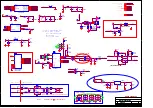
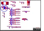
U24
PS321
SPQFP80/SMD
U24
PS321
SPQFP80/SMD
PC0
/I2
C_
RST
1
SDA1
2
SCL
1
3
GND
4
B1
1
5
A1
1
6
VCC
7
B1
2
8
A1
2
9
GND
10
B1
3
11
A1
3
12
VCC
13
B1
4
14
A1
4
15
GND
16
VCC
17
REXT
18
NC
19
PC1
/PO
WDN
20
S1/SDA_CTL
21
S2/SCL_CTL
22
S3/I2C_ADDR
23
GND
24
Y4
25
Z4
26
VCC
27
Y3
28
Z3
29
GND
30
Y2
31
Z2
32
VCC
33
Y1
34
Z1
35
GND
36
I2C_CTL_EN
37
SCL_SINK
38
SDA_SINK
39
HPD_SINK
40
PO
W_
SI
NK
41
OE
/S
T
B
42
PO
W3
43
HPD3
44
SDA3
45
SCL
3
46
GND
47
B3
1
48
A3
1
49
VCC
50
B3
2
51
A3
2
52
GND
53
B3
3
54
A3
3
55
VCC
56
B3
4
57
A3
4
58
GND
59
CEXT
60
POW2
61
HPD2
62
SDA2
63
SCL2
64
EDID_BRG_EN
65
GND
66
B21
67
A21
68
VCC
69
B22
70
A22
71
GND
72
B23
73
A23
74
VCC
75
B24
76
A24
77
GND
78
POW1
79
HPD1
80
R2050
0
R2050
0
R2121
10K
R0603/SMD
R2121
10K
R0603/SMD
D216
BAV70
D216
BAV70
1
2
3
R2091
1K
R0603/SMD
R2091
1K
R0603/SMD
D211
D211
1
2
R2084
0
R0603/SMD
R2084
0
R0603/SMD
R2124
68R
R2124
68R
D208
D208
1
2
D205
D205
1
2
D197
D197
1
2
+
C710
10uF/16V
+
C710
10uF/16V
D7
NC/SCHOTTKY DIODE/B340A
1N4148/SMD
D7
NC/SCHOTTKY DIODE/B340A
1N4148/SMD
R2049
68R
R2049
68R
R2081
100
R0603/SMD
R2081
100
R0603/SMD
CB145
0.1uF
CB145
0.1uF
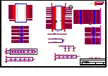
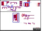
U8
EEPROM 24C02
SOP8/SMD
U8
EEPROM 24C02
SOP8/SMD
NC
1
NC
2
NC
3
GND
4
SDA
5
SCL
6
WP
7
VCC
8
D215
BAV70
D215
BAV70
1
2
3
D203
D203
1
2
TP44
TP44
D8
NC/SCHOTTKY DIODE/B340A
D/SMA/SMD
D8
NC/SCHOTTKY DIODE/B340A
D/SMA/SMD
C
727
100nF
C0402/SMD
C
727
100nF
C0402/SMD
D200
D200
1
2
R2078
4.7K
R0603/SMD
R2078
4.7K
R0603/SMD
R2047
68R
R2047
68R
R2079
47K
R0603/SMD
R2079
47K
R0603/SMD
U13K
MT5380 SMD LQFP
U13K
MT5380 SMD LQFP
OPWR0_5V
73
EXT_RES
77
RX0_CB
79
RX0_C
80
RX0_0B
81
RX0_0
82
RX0_1B
83
RX0_1
84
RX0_2B
85
RX0_2
86
AVDD33_HDMI
78
AVDD12_CVCC
74
R2075
4.7K
R2075
4.7K
R2089 100
R0603/SMD
R2089 100
R0603/SMD
R86
10K
R0603/SMD
R86
10K
R0603/SMD
CB141
0.1uF
C0402/SMD
CB141
0.1uF
C0402/SMD
R2048
68R
R0603/SMD
R2048
68R
R0603/SMD
R2097
47K
R0603/SMD
R2097
47K
R0603/SMD
R2086
37K
R2086
37K
U4
PS331
U4
PS331
HPD2
1
SDA2
2
SCL2
3
B21
4
A21
5
POW2
6
B22
7
A22
8
GND
9
B23
10
A23
11
VCC
12
I2_R
S
T
17
SDA1
18
SCL
1
19
B1
1
20
A1
1
21
VCC
22
B1
2
23
A1
2
24
GND
25
B1
3
26
A1
3
27
NC
28
Z4
37
VCC
38
Y3
39
Z3
40
GND
41
Y2
42
Z2
43
HPD_SINK
44
Y1
45
Z1
46
SCL_SINK
47
SDA_SINK
48
B3
1
53
A3
1
54
PO
W3
55
B3
2
56
A3
2
57
GND
58
B3
3
59
A3
3
60
VCC
61
B3
4
62
A3
4
63
CEXT
64
B24
13
A24
14
POW1
15
HPD1
16
Y4
36
I2C_ADDR
35
SCL_CTL
34
SDA_CTL
33
B1
4
29
A1
4
30
REXT
31
PO
WDN
32
SCL
3
52
SDA3
51
HPD3
50
PO
W_
SI
NK
49
C
726
100nF
C0402/SMD
C
726
100nF
C0402/SMD
D212
D212
1
2
R2080
47K
R0603/SMD
R2080
47K
R0603/SMD
D209
D209
1
2
R2045
100K
R2045
100K
D206
D206
1
2
FB35
FB
FB35
FB
R2094
500%1
R0603/SMD
R2094
500%1
R0603/SMD
C160
10PF/NC
C0402/SMD
C160
10PF/NC
C0402/SMD
C161
10PF/NC
C0402/SMD
C161
10PF/NC
C0402/SMD
R2065
1K/NS
R2065
1K/NS
R2044
0
R2044
0
C
719
100nF
C0402/SMD
C
719
100nF
C0402/SMD
R2098
47K
R0603/SMD
R2098
47K
R0603/SMD
C79
1uF
C79
1uF
R2125
47K
R2125
47K
R2119
1K
R2119
1K
D204
D204
1
2
Q46
2N3904
SOT23/SMD
Q46
2N3904
SOT23/SMD
1
3
2
CN9
10X2 2mm
CN9
10X2 2mm
1
3
5
7
9
11
13
15
2
4
6
8
10
12
14
16
17
19
18
20
C
716
100nF
C0402/SMD
C
716
100nF
C0402/SMD
D201
D201
1
2
R2077
37K
R2077
37K
R2082
1K
R0603/SMD
R2082
1K
R0603/SMD
R2095
4.7K/NC
R0603/SMD
R2095
4.7K/NC
R0603/SMD
D198
D198
1
2
+
C711
10uF/16V
+
C711
10uF/16V
R1606
0R
R0603/SMD
R1606
0R
R0603/SMD
C
720
100nF
C0402/SMD
C
720
100nF
C0402/SMD
R2099
47K
R0603/SMD
R2099
47K
R0603/SMD
C77
4.7uF
C77
4.7uF
FB20
FB
FB20
FB
D6
NC/SCHOTTKY DIODE/B340A
1N4148/SMD
D6
NC/SCHOTTKY DIODE/B340A
1N4148/SMD
R2092
100/NC
R0603/SMD
R2092
100/NC
R0603/SMD
R2120
100K
R2120
100K
C
721
100nF
C0402/SMD
C
721
100nF
C0402/SMD
D210
D210
1
2
Summary of Contents for HL22FEP1
Page 13: ...13 ...
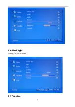
Page 43: ...5 8 6 Backlight Backlight adjust the backlight 8 7 Function ...