5
5
4
4
3
3
2
2
1
1
D
D
C
C
B
B
A
A
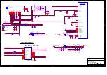
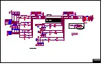
Supply Bypass, A/D Converter
Power and Ground 2
B2
Sabercat
B
14
17
Thursday, May 10, 2007
760_B2.DSN
Title
Size
Document
Rev
Date:
Sheet
of
Drawn by: O. Marinovsky
VCC3_9883
VCC3_9883
VCC3_9883
PLL_PVD
FIL_VDD
FIL_VCC
FIL_VDD
PLL_PVD
FIL_VCC
U8B
AD9883A
39
42
45
46
51
52
59
62
11
22
23
69
78
79
26
27
34
35
1
10
20
21
24
25
28
32
36
40
41
44
47
50
53
60
61
63
68
80
VD
VD
VD
VD
VD
VD
VD
VD
VDD
VDD
VDD
VDD
VDD
VDD
PVDD
PVDD
PVDD
PVDD
GND
GND
GND
GND
GND
GND
GND
GND
GND
GND
GND
GND
GND
GND
GND
GND
GND
GND
GND
GND
TP98
FB10
150_Ohm_600mA
1
2
FB11150_Ohm_600mA
1
2
C359
0.1uF
C360
0.1uF
C365
0.1uF
+
C358
10uF/16V
+
C363
10uF/16V
C362
0.1uF
C353
0.1uF
FB9
150_Ohm_600mA
1
2
C355
0.1uF
C357
0.1uF
C361
0.1uF
C354
0.1uF
C366
0.1uF
C364
1uF
C356
0.1uF
Summary of Contents for HL32S-A
Page 1: ...HL32S A...
Page 5: ...Safety Precautions...
Page 7: ...b Printed Circuit IC Board 1 head on board...
Page 8: ...2 rear board...
Page 9: ...Key IC Description Trouble Shooting Guide 1 Key IC Description 1 ZORAN39760...
Page 10: ...2 HYB25DC256163CE 4...
Page 11: ...3 AD9883...
Page 12: ...4 M25P32...
Page 13: ...2 Trouble Shooting Guide...
Page 16: ...2 SW SW This is the current software version...
Page 17: ...2 Aging Mode This is for factory run in testing...
Page 18: ...3 RF Upgrade is for debugging and do not change anything commonly...
Page 19: ...4 Service Menu is for debugging and do not change anything commonly...
Page 21: ...2 Others...
Page 22: ......
Page 23: ......
Page 24: ...Circuit Diagram 1 BCM signal flowing chart 2 Circuit Diagram...
Page 43: ...Connection Sketch Interpretat...
Page 44: ......

