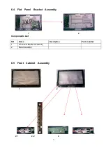
background image

A

A

B

B

C

C

D

D

E

E

4

4

3

3

2

2

1

1

LVDS OUT

LO = > LVDS  POWER OFF

HI = > LVDS  POWER ON

2A

SELECT Low For Internal

FOR CHI-MEI INVERTER

CONNECTOR

Back Light circuit

SELECT Hi  For External

Inverter_Control

FOR PDP DISPLAY

ENABLE

FOR LVDS FORMATE SELECT

M80_PWN

M80_PREST

M80_INTO

M80_POWER

M80_CLK

MT5380P1-V2

V1

C

9

15

Wednesday, January 30, 2008

LVDS/MUTE

NUSTC_5380P1_V2:HAIER

Title

Size

Document Number

Rev

Date:

Sheet

of

Drawn

+5V
AV33

AVDD33_VPLL

+12V

GPIO_9

GPIO_[4..11]

AVDD33_LVDS
AVDD33_LVDS

CK1P

A3P

A3N

A4N
A4P

A2N
A2P
CK1N

A0P

A0N

A1P

A1N

AVDD33_LVDS

AVDD33_VPLL

+3V3SB

+5V

DV33

SELECT

OPWM1

OPCTRL2

BL_ON/OFF

+12V

OPCTRL2

OPWM[1..2]

+5VSB

GND

A3N

A2N

A0N

CK1N

A1N

LVDSVDD

A1P

A0P

CK1P

A2P

A3P

LVDSVDD

GPIO_10

GPIO_11

AVDD33_LVDS

CK2P

CK2N

A5P

A4N

A6N

A4P

A5N

A6P

A7N

A7P

A5N
A5P
A6N
A6P

A7N
A7P

CK2N

CK2P

OSDA0

DIMMING_OUT

DIMMING_OUT

Dimming

OSDA0

U2TX

U2RX

ADIN4

OPWM0

VCXO

AOMCLK

OSDA0

U2RX

U2TX

OPWM0

VCXO

ADIN4

AOMCLK

A0SDATA0

OSCL0

OSCL0

OSCL0

A0SDATA0

A4N

GND

LVDSVDD

A4P

LVDSVDD

LVDSVDD

OPWM1

GND

1,2,3,4,5,6,7,8,10,11,12,13,14,15

+5V

1,2,3,5,8,10,13,14,15

AV33

2,3,5,8,10,13

+12V

1,3,10,14,15

GPIO_[4..11]

4,8,13,14,15

+3V3SB

1,2,4,7,8,13

+5V

1,2,3,5,8,10,13,14,15

+12V

1,3,10,14,15

OPCTRL2

4

OPWM[1..2]

4,7

+5VSB

1,2,11,13,15

GND

1,2,3,4,5,6,7,8,10,11,12,13,14,15

DV33

2,4,7,14

U2RX

7,9,12

U2TX

7,9,12

OSDA0

4,9

OPWM0

4,9

VCXO

4,9

ADIN4

4,9

AOMCLK

13

A0SDATA0

13

OSCL0

4,9

+12V

AV33

AV33

+5V

+3V3SB

DV33

+5V

+5V

+5V

+12V

+3V3SB

+5V

+3V3SB

+12V

+3V3SB

DV33

+5V

+3V3SB

R2109

100

R410
10k

R0603/SMD

R2110

100

R48

NC

R0603/SMD

R47

NC

R0603/SMD

+

CE652

470uF/16v 

TP45

TP/SMD/D0.6

CB155
0.1uF

C0603/SMD

CB216
0.1uF

C0603/SMD

CB1007
0.1uF

C0603/SMD

TP46

TP/SMD/D0.6

L153

NC/FB

R1206/SMD

R2103
10K

Q9
2N3904

SOT23/SMD

1

3

2

R2106

100

Q29
2N3904

SOT23/SMD

1

3

2

R2096

NS/0

R123

100K

R0603/SMD

L132

FB

R1206/SMD

U76
AP1530/SOP-8

SOP8/SMD

1

2

3

4

5

6

7

8

FB

EN

OCSET

Vcc

O/P

O/P

Vs

s

Vs

s

+

CE72
100uF/16V

C100UF16V/D6.3H7

R2105

100

R401
10K

R0603/SMD

FB12

NC

R1206/SMD

Q28
2N3904

SOT23/SMD

1

3

2

C85
1uF

C0603/SMD

R2102
10K

R2072
4.3K

R0603/SMD

U13C

MT5380 SMD LQFP

LQFP256/SMD/5380

244
243
242
241
239
238
237
236
235
234
233
232
230
229
228
227
226
225
224
223

222
231
240

219

220
221

A0N
A0P
A1N
A1P
A2N
A2P
CK1N
CK1P
A3N
A3P
A4N
A4P
A5N
A5P
A6N
A6P
CK2N
CK2P
A7N
A7P

AVDD33_LVDSA
AVDD33_LVDSB
AVDD33_LVDSC

AVDD33_VPLL

TP2
TN2

R400
10k

R0603/SMD

CND1

A2006WV0-16X2

DIP16X2/P2.0

1

2

3

4

5

6

7

8

9

10

11

12

13

14

15

16

17

18

21

20

19

22

23

24

25

26

27

28

29

30

31

32

R408
10K

R0603/SMD

R392

1K

R0603/SMD

FB37

FB

BEAD/SMD/0603

CN5

8X2 2mm

1

3

5

7

9

11

13

15

2

4

6

8

10

12

14

16

D214
SCHOTTKY DIODE/B340A

D/SMA/SMD

R397
0

R0603/SMD

R125

51k

R0603/SMD

R46

4.7K

R0603/SMD

R124
1K

R0603/SMD

+

CE580

100uF/16V

C100UF16V/D6.3H7

CNE4

PH-6A

SIP-6P-2.0A

1
2
3
4
5
6

R2101

100

R2074
820

R0603/SMD

QF3

FDS9435

SMD/SOP8/P1.27

1
2
3
4

5

6

7

8

C86
4.7uF/10V

C0805/SMD

R407
NS/10K

R0603/SMD

R2073
100K

R0603/SMD

CN1

PH-4A

SIP-4P-2.0A

1
2
3
4

CB152
0.1uF

C0603/SMD

R23 0

R391

NS/1K

R0603/SMD

R2107

100

Q26
2N3904

SOT23/SMD

1

3

2

C730
NC/100nF

C0603/SMD

R2104

100

R409

4.7k

R0603/SMD

FB55

FB

BEAD/SMD/0603

+

CE71
220uF/16v

C220UF10V/D6.3H7

R404

4.7k

R0603/SMD

R2071
3K

R0603/SMD

R24 0

CB192
0.1uF

C0603/SMD

C106
1uF

C0603/SMD

+

CB455
10uF/16V

C33UF16V/D5H7

CB217
0.1uF

C0603/SMD

CB992
1uF

C0603/SMD

CB154
0.1uF

C0603/SMD

CNE3

1

2

3

4

5

R399
NC

R0603/SMD

R406
NS/10K

R0603/SMD

CB213
1uF

C0603/SMD

+

CE651

100uF/16V

C100UF16V/D6.3H7

R2108

100

+

CE49
220uF/16V

C220UF10V/D6.3H7

+

CE52

470uF/16V

C470UF16V/D8H9

R396

4.7k

R0603/SMD

L1

33uH/POWER CHOKE

L5-9

R2111

100

C731
100nF

C0603/SMD

R394

10k

R0603/SMD

Summary of Contents for L32K1

Page 1: ...1 HL32K MTK5380 Panel T315XW02_VL AU Chassis MTK5380 2008 Haier Electronic Company Limited All rights reserved Unauthorized copying and distribution is a violation of law...

Page 2: ...warnings or cautions to advise non technical individuals of potential dangers in attempting to service a product Products powered b electricity should be serviced or repaired only by experienced profe...

Page 3: ...s 21 5 2 Back panel controls 22 5 3 Setting Up Your Remote Control 23 6 DISASSEMBLY INSTRUCTIONS 24 6 1 THE UNIT 25 6 2 Support Stand Subassembly 26 6 3 Back Cabinet Assembly 26 6 4 Flat Panel Bracket...

Page 4: ...not use your TV near water For example do not use it near a bath tub wash bowl kitchen sink laundry tub in a wet basement or near a swimming pool Cleaning Unplug your TV before cleaning Do not use li...

Page 5: ...from lightning and power line surges Servicing Do not attempt to service your TV yourself because opening or removing covers may expose you to angerous voltage or other hazards Refer all servicing to...

Page 6: ...ransistors which provide exceptionally sharp video quality Occasionally a few non active pixels may appear on the screen as a fixed blue green or red point These non active pixels do not adversely aff...

Page 7: ...7 3 LOCATION OF CONTROLS AND COMPONENTS 3 1 Board Location No Parts number Description A Board Mainboard Assembly B Board Power Supply Board Assembly 3 2 Mainboard Assembly...

Page 8: ...8 3 2 1 Function Description Mainboard Assembly Process signal which incept from exterior equipment then translate into signal that panel can display Signal flowing chart MTk5380...

Page 9: ...Ground 3 5VSB Power of TV standby 4 GND Ground 5 GND Ground 6 12V Power of system 7 12V Power of system Pin number Signal name Description 1 5V Supply the Power of bright and IR receiver 2 IR Receive...

Page 10: ...V Not use Pin number Signal name Pin number Signal name Pin number Signal name 1 LVDS VDD 9 Not use 17 A1P 2 LVDS VDD 10 Not use 18 A1N 3 LVDS VDD 11 Not use 19 A2P 4 LVDS VDD 12 Not use 20 A2N 5 Not...

Page 11: ...NGAL 12 RO 1 N ODD LVDS SINGAL 13 RO 1 P ODD LVDS SINGAL 14 RO 2 N ODD LVDS SINGAL 15 RO 2 P ODD LVDS SINGAL 16 GND GND 17 ROCLK ODD LVDS SINGAL 18 ROCLK ODD LVDS SINGAL 19 GND GND 20 RO 3 N ODD LVDS...

Page 12: ...9 10 GND Ground 11 NC NC 12 BLON BL ON OFF 13 PWM Internal PWM Control 14 NC NC 4 INSTALLATION INSTRUCTIONS 4 1 External Equipment Connections Accessories Antenna Connection Generally speaking to enjo...

Page 13: ...Choose Your Connection There are several ways to connect your television depending on the components you want to connect and the quality of the signal you want to achieve The following are examples o...

Page 14: ...14...

Page 15: ...15...

Page 16: ...16...

Page 17: ...17...

Page 18: ...solution appropriately To get the best picture quality adjust the output resolution of the source device to 1280x720p Select HDMI input source in input source option of Select Main source menu When th...

Page 19: ...19 HDMI Cable not supplied with the product HDMI to DVI Cable not supplied with the product Analog Audio Cable Stereo to RCA type not supplied with the product...

Page 20: ...20 Power source Removing the table stand and installing a wall mount bracket...

Page 21: ...as left right buttons 4 CH Press to scan through channels To scan quickly through channels press and hold down either In the MENU screen these buttons serve as up down buttons 5 POWER Press to turn o...

Page 22: ...nect digital audio from an external device NOTE In standby mode these ports will not work 8 VIDEO Out Connect the second TV or monitor to the TV s AV OUT 9 AUDIO Out Connect the audio L R cables to th...

Page 23: ...the remote control to shock or liquids Do not use the remote control in an area with high humidity Do not place the remote control in direct sunlight Do not place objects such as furniture between th...

Page 24: ...er indicated with Then remove the Support Stand 2 Remove the Back Cabinet Remove the twelve screws indicated on figure above by Then remove the Back Cabinet from the unit 3 Remove the Mainboard Rmove...

Page 25: ...el Power Supply Board Assembly Harness Assembly Components List NO Name Description Parts number 1 Accessories Assembly 2 Packaging Assembly 3 TV Set 3 1 Support Stand Assembly 3 2 Back Cabinet Assemb...

Page 26: ...n Parts number 2 Support Stand Assembly 3 Bolt SQH 3503RFE Q 6 3 Back Cabinet Assembly 1 2 NO Name Description Parts number 1 Back Cabinet Assembly 2 1 Back Cabinet Subassembly 2 2 Side AV Instruction...

Page 27: ...27 6 4 Flat Panel Bracket Assembly 1 2 Components List NO Name Description Parts number 1 Flat Panel Bracket Assembly 2 Metal Assembly 6 5 Front Cabinet Assembly 1 2 3 2 1 2 2 4...

Page 28: ...oard Assembly 6 6 Harness Assembly 6 6 1 Wire Photo 6 6 2 Components List NO Name Description Parts number 1 Key wire PH 3 800mm PH 3 2 Remote control wire PH 5 300 PH 5 3 Combine wire TJC3 7A 150 TJC...

Page 29: ...7 MEASUREMENTS AND ADJUSTMENTS The way to the factory mode menu 1st press the manu button 2en input 8893 Finished these operations system will be into the factory mode menu 1 Version Info 2 Video 3 Au...

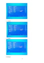
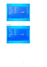
Page 30: ...30 4 Channel 5 Gamma 6 BackLight...

Page 31: ...31 7 Function...

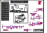
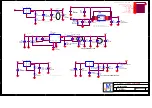
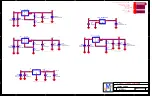
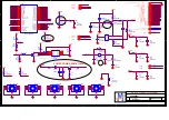
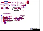
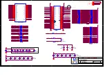
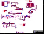
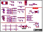
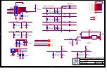
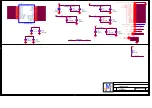
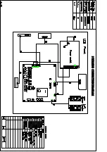
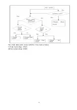
Page 32: ...32 8 BLOCK DIAGRAM AND CIRCUIT DIAGRAM 8 1 BLOCK DIAGRAM 8 2 CIRCUIT DIAGRAM MTK5380...

Page 33: ...TPA1301 U17 U18 5V 12V 0 8 x 1 12K 2 2K 5 1V HDMI2 MT5380P1 V2 V1 C 1 15 Wednesday January 30 2008 INDEX MAIN POWER NUSTC_5380P1_V2 HAIER Title Size Document Number Rev Date Sheet of Drawn 3V3SB 5VSB...

Page 34: ...OP8 SMD 1 2 3 4 5 6 7 8 GND SD VSENSE VREF VDDQ AVIN PVIN VTT R519 100K R0603 SMD R2 2K R0603 SMD R1 110 R0603 SMD CB64 0 1uF C0603 SMD U11 LT1084 TO 252 3 TO 252 3 SMD 3 1 2 IN ADJ GND OUT R11 180 R0...

Page 35: ...1uF C0603 SMD CE96 220uF 16V C220UF10V D6 3H7 R14 180 R0603 SMD CB228 0 1uF C0603 SMD CB197 0 1uF C0603 SMD R19 0 R0603 SMD C575 1uF C0603 SMD CB229 0 1uF C0603 SMD CE19 470uF 16V C470UF16V D10H9 CE22...

Page 36: ...603 SMD C21 5pF C0603 SMD R22 47K R0603 SMD R198 10K R0603 SMD R40 4 7K R0603 SMD C22 1uF C0603 SMD R27 1 R0603 SMD CB2 0 1uF H3 HOLE GND 2 3 4 5 9 8 7 6 1 2 3 4 5 9 8 7 6 1 FB17 FB BEAD SMD 0603 R42...

Page 37: ...AFT NC or IF_AGC Mon NC or B2_Ana_ 5V TU_ 32V GND GND SCL SDA AS B_IF O P D_IF_AGC NC D_IF_O P_1 D_IF_O P_2 CB450 NS 100pF C0603 SMD C41 1uF C0603 SMD C42 0 01uF C0603 SMD C70 10nF C0603 SMD CE38 100...

Page 38: ...03 SMD CA5 0 1uF C0402 SMD RA8 75 R0603 SMD RNA4 47x4 RN0402 SMD 1 2 3 4 5 6 7 8 RA7 75 R0603 SMD RNA6 47x4 RN0402 SMD 1 2 3 4 5 6 7 8 RA14 100 R0603 SMD CA27 0 1uF C0603 SMD UA1 16M x 16 DDR TSOP 66...

Page 39: ...D R1257 NC 4 7K R0603 SMD R45 4 7K R0603 SMD R54 10K R0603 SMD R61 4 7K R0603 SMD U17 M25P16 NS CASON8 SMD 1 2 3 4 5 6 7 8 S_ Q W_ VPP VSS D C HOLD_ VCC R1703 100R R0603 SMD R1705 100R R0603 SMD R1227...

Page 40: ...C0805 SMD D211 PESD1206Q 140 PESD1206Q 140 SMD 1 2 3 4 5 6 7 8 R2116 68R R2050 0 C720 100nF R2113 100K R2092 100 NC R2065 1K NS R2080 47K C725 100nF CN2 HDMI HAIER 20 21 1 2 3 4 5 6 7 8 9 10 11 12 13...

Page 41: ...9 2N3904 SOT23 SMD 1 3 2 R2106 100 Q29 2N3904 SOT23 SMD 1 3 2 R2096 NS 0 R123 100K R0603 SMD L132 FB R1206 SMD U76 AP1530 SOP 8 SOP8 SMD 1 2 3 4 5 6 7 8 FB EN OCSET Vcc O P O P Vss Vss CE72 100uF 16V...

Page 42: ...363 10nF C0603 SMD C353 15pF C0603 SMD R1640 75 R0603 SMD R1836 10K R0603 SMD R1636 68 R0603 SMD R1878 1K R0603 SMD C636 4 7uF 6 3V C0603 SMD R1842 10K R0603 SMD R36 22 R0603 SMD D157 NS EZJZ0V800AA E...

Page 43: ...FB68 80 100MHz BEAD SMD 0603 C135 10nF C0603 SMD D31 NS EZJZ0V800AA ESD0603 SMD 1 2 R169 68 R0603 SMD R160 0 R0603 SMD R181 0 R0603 SMD R171 75 R0603 SMD R182 10K R0603 SMD C137 5pF C0603 SMD R161 0 R...

Page 44: ...0603 SMD L34 0 L IND SMD 0603 C459 47pF C0603 SMD R1525 47 R0603 SMD R79 100 R0603 SMD D147 NS EZJZ0V800AA ESD0603 SMD 1 2 C111 NS 43pF C0603 SMD w red P80 RCA2X1 RCA2 HAIER 1 3 5 4 2 R1560 100 R0603...

Page 45: ...15 OFF_MUTE 14 AOLRCK 7 AOBCK 7 GPIO_ 4 11 4 8 9 14 15 OPCTRL1 4 11 3V3SB 1 2 4 7 8 9 AR2 14 AL2 14 HPDET 14 AIN3_L 10 AIN3_R 10 5VSB 1 2 11 15 GND 1 2 3 4 5 6 7 8 9 10 11 12 14 15 A0SDATA0 9 AOMCLK...

Page 46: ...16V C220UF16V D6H11 C659 4 7uF 6 3V C0603 SMD CE20 220uF 16v C220UF16V D6H11 R1800 10K R0603 SMD C40 1uF C0603 SMD C167 2 2nF R64 R1766 20K R0603 SMD CB981 0 1uF C0603 SMD R1767 20K R0603 SMD D16 NS...

Page 47: ...4 7K R0603 SMD R1781 4 7K_DNS R0603 SMD C681 0 22uf C0603 SMD C665 0 22uf C0603 SMD R1785 470 R0603 SMD 1 2 R1773 39K R0603 SMD R1777 4 7K R0603 SMD CE630 47uF 16V C47UF16V D5H7 1 2 R1784 NC R0603 SMD...

Page 48: ......

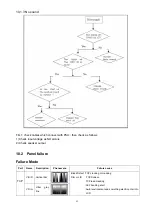
Page 49: ...49 10 TROUBLE SHOOTING GUIDE 10 1 Simple check 10 1 1 PDP is not bright 10 1 2 No picture...

Page 50: ...50 First check cables which connect with PSU then check as follows 1 Check input voltage CNA1 2 Check output voltage CND1...

Page 51: ...O picture 2 Check speaker output 10 2 Panel failure Failure Mode Part Name Description Phenomena Failure cause V B D Vertical bar TCP V Dim Virtal gray line Block Defect TCP cracking or cracking Dim o...

Page 52: ...Bubble Bladder in Polarizer Bladder between Polarizer and top glass Polarizer Scratch Polarizer Scratch Tine or rigidity arose Panel or Polarlzer F M inside Polarizer Eyewinker inside Polarizer Eyewi...

Page 53: ...l Nolse When turn panel appear cacophony Caused by Mechanica noise of backlight unit Ripple Connectric circle Causeed by between mechanism and Panel B L off B L lose action Connect badness between wir...

Page 54: ...Mode Part Name Description Phenomena Failure cause Light leakage Brightness at bottom of LCM brighter than normal B L unit badness Uniformity B L brightness asymmetric Sheet in B L unit is uneven Mech...

Reviews: