- 13 -
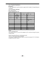
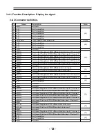
43 GND
Ground
44 GND
Ground
45 GND
Ground
46 GND
Ground
47 N.C.
No Connection
(2)
48 VCC
Power input (+12V)
49 VCC
Power input (+12V)
50 VCC
Power input (+12V)
51 VCC
Power input (+12V)
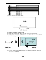
Note (1) LVDS connector pin order defined as follows.
Note (2) Reserved for internal use. Please leave it open.
Note (3) Low = Open or connect to GND: VESA Format, High = Connect to +3.3V: JEIDA Format.
Note (4) LVDS signal pin connected to the LCM side has the following diagram. R1 in the system side should be
less than 1K Ohm. (R1 < 1K Ohm)
TCON
R2
R1
Setting
Selector (pin7)
LCM side
System side
R3
TCON
R2
R1
Setting
LCM side
System side
R3
Note (5) Two pixel data send into the module for every clock cycle. The first pixel of the frame is odd pixel and
the second pixel is even pixel
Summary of Contents for LEC32B1380
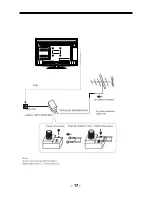
Page 18: ... 17 ...
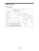
Page 26: ...7 Electrical parts 7 1 Block diagram 25 AMP Headphone Coaxial 1 2 MSD318QT Main IC ...
Page 37: ...8 TV OPERATION 36 ...
Page 38: ... 37 ...
Page 39: ... 38 Press ENTER Key To Select ...
Page 40: ... 39 Press ENTER Key To Select ...
Page 41: ... 40 ...
Page 44: ... 43 9 Trouble shooting 9 1 Simple check ...
Page 46: ... 45 3 Panel display abnormally connector J9 is at normal level ...


