27
The case-change code is coupled through a NAND gate (part of IC-25) and an inverter to IC-33, where it
is used in place of the shift register output to control the keying circuit.
When the keyboard is switched to the Morse mode, the
M/R
bus goes low. Since this signal is coupled to
pin 10 of IC-33 and Pin 10 of IC-55, the outputs of both these gates remain high. Clock pulses are thus
allowed to flow to the keying circuit, and the RTTY loop is held in the mark state. One section of the mode
switch, S301B, also shorts across the loop keying contacts in the Morse mode as a means of completing the
loop circuit when the keyboard power is switched off.
4.10 RTTY Timing Chain
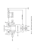
Accurate timing pulses for RTTY operation are derived from four crystal-controlled oscillators, one for
each RTTY speed, as shown in Figure 8.8. The outputs of the oscillators are fed to four separate NAND
gates. Only one of the gates is enabled at any time, as determined by the setting of the mode switch,
S301A.
The gate outputs are coupled through a NOR gate, composed of four open collector inverters (part of IC-
30), to the input of a sixteen-bit binary counter. Consequently, the clock signal appropriate to the RTTY
operating speed chosen is supplied to the counter.
The first four stages of the counter, which divide the input frequency by a factor of sixteen, drive the
VHØ clock line. This signal, in the range from about 375 to 610 kHz (depending on the operating speed), is
used in the RTTY loop interface (Figure 8.7) to drive the isolation circuit during mark pulses. It is also
supplied to the quick brown fox generator to clear the circuit rapidly in the Morse mode.
In the next four counter stages, the frequency is again divided by sixteen to obtain the HØ clock signal,
which toggles at 512 times the baud rate. The HØ clock line synchronizes operation of the keyboard encoder
(Figure 8.3) with the buffer control and the shift register control circuits (Figures 8.4 and 8.6, respectively).
The HØ clock signal is again divided by the remaining eight counter stages to produce the Ø clock signal
at twice the baud rate. The reset terminals of the last four stages are controlled by the
RTTY START
line,
which clears the flip-flops between characters and allows clock pulses to flow only after a character has
been transferred from the storage buffer to the shift register. The reset feature also ensures that the first
shift of the register will occur exactly one select-pulse duration after the beginning of the start pulse.
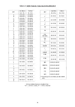
Table 4.1 lists the frequencies of the four oscillators, as well as the corresponding VHØ, HØ and Ø clock
frequencies for each RTTY speed.
Also shown in Figure 8.8 is the circuit which drives the M/R and the
M/R
lines. In the RTTY mode, the
input to an inverter (pin 9 of IC-30) is pulled high by resistor R21, which is connected to the +5 Volt supply
bus. The
M/R
line is therefore high and the M/R bus is driven low. Conversely, when the switch is moved_to
the Morse position, the inverter input is grounded, pulling the
M/R
bus low and allowing the M/R line to go
high.
Table 4.1: RTTY Timing Chain Output Frequencies
RTTY
Operating
Speed (WpM)
Oscillator
Frequency
(kHz)
VHØ
Clock Rate
(kHz)
HØ
Clock Rate
(kHz)
Ø
Clock Rate
(kHz)
100
9730.660
608.166
38.010
148.478
75
7459.988
466.249
29.141
113.830
66
6553.600
409.600
25.600
100.000
60
5957.818
372.364
23.273
90.909
Supplied to other portions of the keyboard circuitry, these signals activate the RTTY control and encoder
circuits in the RTTY mode, and the Morse character generator and output control circuits in the Morse mode.
They also control the input to the shift register, determine the character code produced in the ROM code
converter, and inhibit the operation of the quick brown fox generator in the Morse mode.
Summary of Contents for DKB-2010
Page 1: ......
Page 20: ...18...
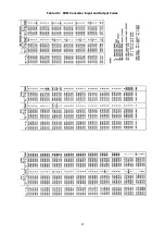
Page 39: ...37 Table 4 3 ROM Converter Input and Output Codes...
Page 52: ...50 Figure 6 1 Logic Circuit Board Test Points...
Page 53: ...51 Figure 6 2 Keyswitch Circuit Board Test Points...
Page 54: ...52 Figure 6 3 Power Supply Circuit Board Test Points...
Page 57: ...55 Table 6 4 DKB 2010 Wire List...
Page 63: ...61...
Page 64: ...62...
Page 65: ...63...
Page 67: ...65...
Page 69: ...67...
Page 71: ...69...
Page 73: ...71...
Page 75: ...73...
Page 77: ...75...
Page 79: ...77...
Page 81: ...79...
Page 83: ...81...
Page 85: ...83...
Page 87: ...85...
Page 89: ...87...
Page 91: ...89...
Page 92: ...90...
Page 93: ...91...
Page 94: ...92...
Page 95: ...93...
Page 96: ...A1 EXTENDED MEMORY OPTION FOR THE DKB 2010 KEYBOARD INSTRUCTION MANUAL...
Page 100: ...A5...
Page 101: ...A6...


