2
ILLUSTRATIONS
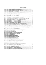
Figure 2.1: Typical Connection for Cathode Keying ........................................ 9
Figure 2.2: Typical Connection for Grid-Block Keying ..................................... 10
Figure 2.3: Typical Loop Circuit Connection .................................................. 10
Figure 2.4: Connection for Loop Circuit with Negative Lead Grounded ............ 11
Figure 2.4a: Plug Preparation ....................................................................... 11
Figure 2.5: Bridge Polarity Protection Circuit ................................................. 12
Figure 3.1: Location of Controls and Keys ..................................................... 14
Figure 4.1: MM5740 Keyboard Encoder Integrated Circuit .............................. 18
Figure 4.2: Shift Register Waveforms for Transmission of the Letter "F" .......... 24
Figure 4.3: Shift Register Control Signals for Morse Operation ........................ 25
Figure 4.4: Generation of the Letters-Shift Code ........................................... 26
Figure 4.5: Generation of the Figures-Shift Code ........................................... 26
Figure 4.6: Morse Clock and Decoder Waveforms .......................................... 29
Figure 4.7: Production of Dots by the Morse Character Generator .................. 29
Figure 4.8: Production of Dashes by the Morse Character Generator ............... 30
Figure 4.9: Suppression of Dot at End of Character to Produce Intercharacter
Space ....................................................................................... 31
Figure 4.10: Development of Clock Pulses for Automatic Character Sequencers 33
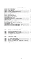
Figure 5.1a: Rear Panel Component Placement
Figure 5.1b: Matching Transformer and Terminal Strip Details
Figure 5.1c: Rear Panel Wiring
Figure 5.1d: Wiring Detail for T301
Figure 5.2: Installation of Power Cord Strain Relief
Figure 5.3a: Top Panel Component Placement
Figure 5.3b: Top Panel Wiring
Figure 5.4: Wiring Harness Placement
Figure 5.5: Assembly of Cabinet End Panels
Figure 5.6: Space Bar mounting detail
Figure 5.7: Integrated Circuit Orientation
Figure 5.8: Mounting the MJE521 Power Transistor
Figure 5.9: Capacitor Placement on Power Supply Board
Figure 5.10: Jumper Placement on Logic Circuit Board
Figure 5.11: Weight-Ratio Jumper Placement
Figure 5.12: Bottom Cover Assembly
Figure 5.13: Assembled DKB-2010 with Bottom Cover Removed
Figure 5.14: Diode Placement in Identifier Matrix ........................................... 44
Figure 6.1: Logic Circuit Board Test Points .................................................... 50
Figure 6.2: Keyswitch Circuit Board Test Points ............................................. 51
Figure 6.3: Power Supply Circuit Board Test Points ....................................... 52
Summary of Contents for DKB-2010
Page 1: ......
Page 20: ...18...
Page 39: ...37 Table 4 3 ROM Converter Input and Output Codes...
Page 52: ...50 Figure 6 1 Logic Circuit Board Test Points...
Page 53: ...51 Figure 6 2 Keyswitch Circuit Board Test Points...
Page 54: ...52 Figure 6 3 Power Supply Circuit Board Test Points...
Page 57: ...55 Table 6 4 DKB 2010 Wire List...
Page 63: ...61...
Page 64: ...62...
Page 65: ...63...
Page 67: ...65...
Page 69: ...67...
Page 71: ...69...
Page 73: ...71...
Page 75: ...73...
Page 77: ...75...
Page 79: ...77...
Page 81: ...79...
Page 83: ...81...
Page 85: ...83...
Page 87: ...85...
Page 89: ...87...
Page 91: ...89...
Page 92: ...90...
Page 93: ...91...
Page 94: ...92...
Page 95: ...93...
Page 96: ...A1 EXTENDED MEMORY OPTION FOR THE DKB 2010 KEYBOARD INSTRUCTION MANUAL...
Page 100: ...A5...
Page 101: ...A6...


