60
VIII. DIAGRAMS
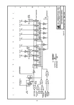
In this section you will find the schematic diagrams and layout drawings for the DKB-2010 keyboard, as
listed below.
An explanation of the labels and codes used in the schematic diagrams may be found in Section 4.3. The
drawing conventions are depicted in Figure 8.2.
Figure 8.1:
DIG-2010 Block Diagram
Figure 8.2:
Drawing Conventions
Figure 8.3:
Keyboard Encoder
Figure 8.4:
ROM Code Converter and Buffer Control
Figure 8.5:
RTTY Control and Decoder
Figure 8.6:
Shift Register Control
Figure 8.7:
RTTY Encoder and Loop Interface
Figure 8.8:
RTTY Timing Chain
Figure 8.9:
RTTY Character Counter
Figure 8.10:
Morse Character Generator
Figure 8.11:
Morse Output Control
Figure 8.12:
Quick Brown Fox Generator and ID Control
Figure 8.13:
Identifier
Figure 8.14:
Three-Character Sequencers
Figure 8.15:
Power Supply Module
Figure 8.16:
Power Supply Board Component Layout
Figure 8.17:
Keyboard Circuit Board Component Layout
Figure 8.18:
Keytop Positions
Figure 8.19:
Main Logic Board Component Layout - IC's
Figure 8.20:
Main Logic Board Component Layout - Small Parts
Summary of Contents for DKB-2010
Page 1: ......
Page 20: ...18...
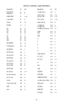
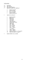
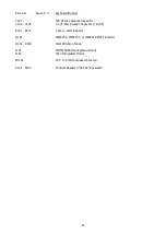
Page 39: ...37 Table 4 3 ROM Converter Input and Output Codes...
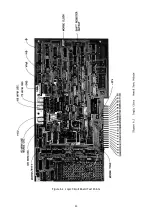
Page 52: ...50 Figure 6 1 Logic Circuit Board Test Points...
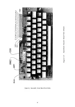
Page 53: ...51 Figure 6 2 Keyswitch Circuit Board Test Points...
Page 54: ...52 Figure 6 3 Power Supply Circuit Board Test Points...
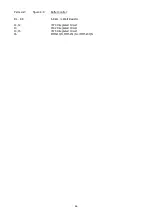
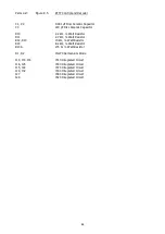
Page 57: ...55 Table 6 4 DKB 2010 Wire List...
Page 63: ...61...
Page 64: ...62...
Page 65: ...63...
Page 67: ...65...
Page 69: ...67...
Page 71: ...69...
Page 73: ...71...
Page 75: ...73...
Page 77: ...75...
Page 79: ...77...
Page 81: ...79...
Page 83: ...81...
Page 85: ...83...
Page 87: ...85...
Page 89: ...87...
Page 91: ...89...
Page 92: ...90...
Page 93: ...91...
Page 94: ...92...
Page 95: ...93...
Page 96: ...A1 EXTENDED MEMORY OPTION FOR THE DKB 2010 KEYBOARD INSTRUCTION MANUAL...
Page 100: ...A5...
Page 101: ...A6...


