background image

A3

7th Reinstall  the  bottom  plate,  sliding  the  front  edge  beneath  the  front  lip  of  the  cabinet.  Fasten  it  in

place with the original screws.

The keyboard and buffer are now ready to operate. Refer to Section 3 for instructions on the use of the

buffer.

3.

Operating Instructions

Three  keys  (CQ,  AUX  and  HERE  IS)  in  conjunction  with  the  SHIFT  keys  control  the  operation  of  the

buffer.

The shifted HERE IS key clears the buffer of its contents. A shifted AUX stops the flow of characters out

of the buffer. The shifted CQ key turns the buffer output on so that the stored characters pass from the

keyboard to the logic circuitry and are transmitted.

It is important to observe the proper sequence of operations when using these keys to control the buffer.

The  SHIFT  key  must  be  pressed  and  held  down  while  one  of  the  control  keys  is  struck.  The  SHIFT  key

should not be released until after the control key is released. Otherwise, the character sequence produced
by the control key in its normal (unshifted) mode will be entered in the memory unintentionally.

When the keyboard is first switched or, it is not possible to predict the states that the buffer memory

stages  will  assume.  It  is  therefore  best  to  type  a  shifted  HERE  IS  to  clear  the  buffer  and  prepare  it  for

incoming keystrokes.

If you wish to use the buffer as an extension of the keyboard's internal three-character memory, type a

shifted CQ. The buffer output will be turned on and the characters you type will pass through the buffer to
the keyboard logic for transmission. If you type faster than the rate at which the keyboard is transmitting,
the additional characters will "stack up" in the buffer and will be passed on to the keyboard logic when it is
ready to receive them.

When the buffer is completely filled, the BUFFER FULL lamp will light. In that case, stop typing until the

keyboard has had a chance to transmit some of the stored characters. As soon as memory space is available
for another keystroke, the BUFFER FULL lamp will go out.

Transmission of the stored keys may be stopped at any time by typing a shifted AUX. The keyboard will

transmit the two characters stored in its internal memory, but will not draw any more characters from the
buffer. To restart transmission, type a shifted CQ. The contents of the buffer may be erased at any time by
typing a shifted HERE IS.

It is possible to use the buffer to store a complete message or character string by typing a shifted AUX

prior to typing the first character of the message. The buffer output will be turned off, and any keystrokes
will be

recorded in the memory but will not be passed to the logic circuits for transmission. When ready to send

the message, type a shifted CQ. Any pauses or gaps which occur when the message is originally typed will

be closed up, as the keystrokes are stacked up sequentially in the buffer. If you wish to erase the memory,
simply  type  a  shifted  HERE  IS.  The  memory  contents  do  not  recirculate;  once  the  message  has  been

transmitted, it is no longer present in the memory. If you wish to repeat the message, it must be typed into
the buffer again.

Since the buffer, in effect, stores keystrokes rather than individual characters, the QBF (quick brown fox

message), HERE IS (identifier message), CQ and AUX keystrokes occupy only a single memory location. It is
therefore possible, for example, to store the QBF message and 63 (or 127) other keystrokes in the memory.
Note  that  the  repeat  feature  of  the  HERE  IS,  CQ  and  AUX  keys  no  longer  functions  when  the  buffer  is
installed.

The  only  keystroke  which  does  not  enter  the  buffer  is  the  "break"  (BRK)  key  function.  The  break  key

operates as usual unless the buffer output has been turned off, in which case it is deactivated and has no
effect.

Summary of Contents for DKB-2010

Page 1: ......

Page 2: ...Please do not return your keyboard or components to the factory until you have sent a letter of notification and have received a written return authorization This warranty is and shall be in lieu of...

Page 3: ...Circuit Analysis 17 4 4 Scanning Keyboard Encoder 19 4 5 ROM Code Converter 20 4 6 Storage Buffer 20 4 7 RTTY Control and Decoding Circuit 21 4 8 Shift Register and Control Circuit 22 4 9 RTTY Encoder...

Page 4: ...t at End of Character to Produce Intercharacter Space 31 Figure 4 10 Development of Clock Pulses for Automatic Character Sequencers 33 Figure 5 1a Rear Panel Component Placement Figure 5 1b Matching T...

Page 5: ...re 8 16 Power Supply Board Component Layout 89 Figure 8 17 Keyboard Circuit Board Component Layout 90 Figure 8 18 Keytop Positions 91 Figure 8 19 Main Logic Board Component Layout IC s 92 Figure 8 20...

Page 6: ...1 Watt RTTY Keyfunctions 10 numeric 0 through 9 26 alphabetic A through Z 15 punctuation marks 3 carriage control keys linefeed carriage return and blank 2 shift keys 1 break key 2 manual case change...

Page 7: ...used for either cathode or gridblock keying but not both simultaneously Transistor ratings Cathode keying Voltage nonconducting 250 V DC Current conducting 150 mA DC Grid block keying Voltage noncond...

Page 8: ...selected by the owner at the time of purchase if not specified it is coded to transmit DX followed by a space For the RTTY operator the DKB 2010 provides automatic transmission of the case shift code...

Page 9: ...or the kit model In the following sections you will find instructions for installing and operating the DKB 2010 Please read them carefully before attempting to use your keyboard Section 4 provides a f...

Page 10: ...k their operation If this preliminary test is satisfactory the keyboard is ready to be connected to your CW transmitter and RTTY loop circuit If the keyboard will be used for both RTTY and Morse opera...

Page 11: ...pin 2 Connect a jumper wire between pins 1 and 3 of the plug Prepare the plug connections as shown in Figure 2 4A Insert the plug into the Morse Output jack on the rear panel of the keyboard A typical...

Page 12: ...rd ratings UNPLUG THE KEYBOARD AND THE STATION LOOP SUPPLY BEFORE TAKING ANY CONNECTIONS A typical station loop circuit is shown in Figure 2 3 A 6 pin plug is used to connect the loop to the keyboard...

Page 13: ...larity must be carefully observed when constructing the circuit and the leads must be properly insulated and positioned so that they do not short together This circuit is not recommended for loops ope...

Page 14: ...the printer is in letters case pressing a letter key followed by a number key should shift it to figures case Typing another letter should return it to letters case After 64 printing characters have...

Page 15: ...d without using the SHIFT key Some punctuation marks appear on the upper half of their keytops To type these characters press either of the two SHIFT keys and hold it down white you strike the desired...

Page 16: ...haracters on paper tape respectively Although the keyboard produces all required figures case and letters case codes automatically a figures FIGS key and letters LTRS key are provided so that you may...

Page 17: ...manner but the RTTY test generator QBF key is inappropriate for Morse transmission and therefore does not function The BLANK key produces the standard eight dot Morse error signal Five double charact...

Page 18: ...ssage the quick brown fox test signal and the special three character memory sequences The remaining key labeled BREAK allows the operator to break the RTTY loop manually or in the Morse mode to key t...

Page 19: ...ULL Some of the labels are overscored indicating that the signal carried by the line is inverted or negative true Thus the BUFFER FULL line is at its high level above 2 4 Volt when a character has bee...

Page 20: ...18...

Page 21: ...sense logic causes the code appearing at the ROM output at that instant to be transferred to the storage buffer The scanning process is dynamic that is the counters are cycled repetitively at a fairl...

Page 22: ...causes the flip flop to change states if the preceding character was in letters case The keyboard then transmits a figures shift code before producing the current character Likewise if the current cha...

Page 23: ...full the line is driven low As soon as the character in the buffer has been accepted by the shift register the BUFFER READ Line is driven low pulling the RESUME ID bus Low also The identifier then pa...

Page 24: ...r generator gates IC 34 to produce the waveforms shown at the bottom of Figure 8 5 Pin 6 of the gate is low during the 0 and 1 states of the counter producing the C 0v1 output Pin 12 is low during the...

Page 25: ...of these circuits is activated depending on the setting of the mode switch and the desired Morse or RTTY output is produced The pattern of bits loaded into the shift register depends on the keyboard m...

Page 26: ...ed to produce many of the characters the ROM code converter is programmed to follow the required bits for each character with an end bit set to the l state with all remaining bits set low For example...

Page 27: ...r in its base circuit During mark pulses the VH clock signal passes through a NAND gate IC 34 and an inverter IC 24 to drive the emitter of a current source transistor Q1 The pulses are coupled throug...

Page 28: ...If the letter shift character is to be sent the LTRS CASE bus goes high enabling the lower gate The FIGS CASE line remains low disabling the upper gate so its output remains high The C 0v1 signal then...

Page 29: ...the baud rate The H clock line synchronizes operation of the keyboard encoder Figure 8 3 with the buffer control and the shift register control circuits Figures 8 4 and 8 6 respectively The H clock si...

Page 30: ...f IC 25 drive the gate output low resetting all stages of the counter After 32 input pulses the counter output goes high after the 64th pulse it goes low again The counter output is fed to the clock i...

Page 31: ...e flip flop is driven by decoder output 4 pin 5 During the next three clock pulses the flip flop does not change states because its J and K inputs are held low After clock pulse 3 however the decoder...

Page 32: ...op is coupled through the gate to the Morse character bus For dashes both flip flops are active and the two output lines are logically added in the gate as shown in trace g of Figure 4 8 At the end of...

Page 33: ...he incoming character pulses The output of the third gate drives the emitter of Q6 a constant current source which in turn drives the transmitter keying transistor Q5 When the gate output is high the...

Page 34: ...START line low If the mode switch is set for RTTY operation the M R line is low also Both signals are coupled to the input of a NOR gate pins 2 and 3 of IC 54 With the key pressed both inputs are low...

Page 35: ...e states the counter stages will assume when the power is first switched on the circuit may start in the active state To clear the counter quickly in the Morse mode the VH clock signal is supplied to...

Page 36: ...a space The other is programmed at the user s option for any desired message The circuit shown in Figure 8 14 is essentially a simpler version of the identifier Each sequencer contains a two bit coun...

Page 37: ...II input code The ROM produces different outputs for Morse and RTTY modes depending on the state of the A7 input bit Both output codes are listed for each character Since some of the characters are no...

Page 38: ...1010 101 0101 101 0110 101 0111 101 1000 101 1001 101 1010 011 0000 011 0000 1 011 0001 010 0001 2 011 0010 010 0010 3 011 0011 010 0011 4 011 0100 010 0100 5 011 0101 010 0101 6 011 0110 010 0110 KE...

Page 39: ...37 Table 4 3 ROM Converter Input and Output Codes...

Page 40: ...0 0 1 1 1 0 1 0 1 1 0 1 1 1 1 1 0 0 1 1 1 0 1 1 1 1 1 0 1 1 1 1 1 BLANK E LF A SPACE S I U CR D R J N F C K T Z L W H Y P Q O B G FIGS M X V LTRS BLANK 3 LF SPACE BELL 8 7 CR 4 5 2 6 1 9 FIGS LTRS No...

Page 41: ...39 Table 4 5 Morse Codes Character Code Character Code A B 1 C 2 D 3 E 4 F 5 G 6 H 7 I 8 J 9 K L M N O P Q R S T __ U AS __ V SK __ W BT __ X AR __ Y KN Z ERROR...

Page 42: ...automatic sequence keys are precoded by inserting diodes at the proper location in the diode matrix on the logic circuit board The diodes are positioned to represent the ASCII code for each character...

Page 43: ...41 Table 5 1 Coding Chart for Identifier Character A0 A1 A2 A3 A4 A5 A6 CQ key AUX key HERE IS key...

Page 44: ...42 Table 5 1 Coding Chart for Identifier Character A0 A1 A2 A3 A4 A5 A6 CQ key AUX key HERE IS key...

Page 45: ...positioned as indicated by Figure 5 14 178 The figure shows how the diodes should be positioned for the CQ key Note that the diodes are inserted into the board from the component side Referring to the...

Page 46: ...r panel Check again that the wiring harness is not pinched between the cover and the cabinet then fasten the cover in place with four 6 32 5 6 screws one at the front lip and three at the rear Assembl...

Page 47: ...ng all pins of a component such as a 14 pin DIP integrated circuit simultaneously Solder wicking essentially very fine copper braid can be used to absorb solder from the pins once the solder has been...

Page 48: ...ections are being changed Note that unplugging the power supply board will disable the supply Measure the 12 Volt supply at the point shown in Figure 6 1 It should read between 10 5 and 13 5 Volt If t...

Page 49: ...the RTTY mode only Use the waveforms in Section IV for comparison to those observed in the unit under test Symptom Keyboard fails to operate at one RTTY speed O K at other speeds and in the Morse Mode...

Page 50: ...carrying ASCII character codes from the keyswitch circuit board to the logic circuit board are interrupted An improperly installed edge connector is one possible cause a defective or incorrectly insta...

Page 51: ...Y Load I16 3 Morse End I17 2 4 Morse Character I18 6 RTTY Load I19 8 DASH I22 8 Insert Case Code I22 5 ____ DOT I23 8 DOT I23 9 Waveform IC Pin 100 WPM Osc I24 4 Letters Case I25 3 4 Figures Case I25...

Page 52: ...50 Figure 6 1 Logic Circuit Board Test Points...

Page 53: ...51 Figure 6 2 Keyswitch Circuit Board Test Points...

Page 54: ...52 Figure 6 3 Power Supply Circuit Board Test Points...

Page 55: ..._ N ID Active to J of buffer P not used R not used S not used T not used U Speed pot V W Weight H X Weight N Y Weight L Z Weight VL ________ 1 QBF Start ___________ 2 HERE IS Start ________ 3 AUX Star...

Page 56: ...D A3 E A8 not used F A1 H A0 J A7 not used K A6 L A5 M A4 _____ N SHIFT to buffer P Ground S not used ____ T Clock U Ready _____ V Enable W 5 Volt X 12 Volt _______ Y CQ Start ________ Z AUX Start Pow...

Page 57: ...55 Table 6 4 DKB 2010 Wire List...

Page 58: ...Ground and Power Connections IC Type Ground 5 Volt 12 Volt MM5213 none 12 16 24 or MM5231 MM5740 2 32 18 7400 7 14 7401 7 14 7402 7 14 7404 7 14 7405 7 14 7410 7 14 7420 7 14 7430 7 14 7442 8 16 7474...

Page 59: ...Resistors 2 100 Watt 2 120 Watt 1 180 Watt 1 220 Watt 3 270 Watt 1 330 Watt 3 390 Watt 1 470 Watt 4 560 Watt 26 1 k Watt 4 1 8 k Watt 1 2 2 k Watt 1 2 7 k Watt 1 3 3 k Watt 1 4 7 k Watt 1 8 2 k Watt...

Page 60: ...22 tinned bar wire 1 36 length no 22 hook up wire 1 9 length no 22 insulated sleeving 1 48 length no 30 Strip eze magnet wire 1 40 length no 22 Multi core solder 2 48 length 2 conductor shielded cabl...

Page 61: ...dapter 1 Space bar torsion bar 1 Keytop Set consisting of 1 Space bar Keytop 1 Blank Keytop 2 Shift Keytops 1 AUX Keytop 1 CQ Keytop 1 HERE IS Keytop 1 KN RETURN Keytop 1 BRK Keytop 1 QBF Keytop 1 BT...

Page 62: ...re 8 5 RTTY Control and Decoder Figure 8 6 Shift Register Control Figure 8 7 RTTY Encoder and Loop Interface Figure 8 8 RTTY Timing Chain Figure 8 9 RTTY Character Counter Figure 8 10 Morse Character...

Page 63: ...61...

Page 64: ...62...

Page 65: ...63...

Page 66: ...1 F Disc Ceramic Capacitor 16 Volt R101 R107 1 k Watt Resistor Q101 MPS3702 MPS3703 or MPS6518 PNP Transistor D101 D138 1N4148 Silicon Diode I101 MM5740AAA N Integrated Circuit I102 7410 Integrated C...

Page 67: ...65...

Page 68: ...66 Parts List Figure 8 4 Buffer Control R1 R8 6 8 k Watt Resistor I1 I2 7474 Integrated Circuit I3 7402 Integrated Circuit I4 I5 7475 Integrated Circuit I6 MM5213 N MM5231 N or MM5203 N...

Page 69: ...67...

Page 70: ...Watt Resistor R11 2 7 k Watt Resistor R12 R13 10 k Watt Resistor R14 8 2 k Watt Resistor R14A 270 Watt Resistor D1 D2 1N270 Germanium Diode I14 I33 I34 7410 Integrated Circuit I16 I25 7400 Integrated...

Page 71: ...69...

Page 72: ...6 Shift Register Control R9 1 k Watt Resistor I7 7474 Integrated Circuit I8 I11 7402 Integrated Circuit I9 I10 7496 Integrated Circuit I12 7404 Integrated Circuit I16 I18 7400 Integrated Circuit I17 7...

Page 73: ...71...

Page 74: ...t Resistor D4 D5 D6 1N4148 Silicon Signal Diode D7 1N4005 Silicon Power Diode Q1 MPS3702 MPS3703 or MPS6518 PNP Transistor Q2 2N5655 or MJE340 NPN Transistor I24 7404 Integrated Circuit I25 I55 7400 I...

Page 75: ...73...

Page 76: ...tt Resistor R29 R32 560 Watt Resistor D8 1N270 Germanium Diode I24 I29 7404 Integrated Circuit I30 7405 Integrated Circuit I35 7402 Integrated Circuit I36 I39 7493 Integrated Circuit S301 5 position 2...

Page 77: ...75...

Page 78: ...apacitor R37 1 k Watt Resistor R38 10 k Watt Resistor I13 74121 Integrated Circuit I19 7404 Integrated Circuit I20 I23 7473 Integrated Circuit I21 7493 Integrated Circuit I25 7400 Integrated Circuit I...

Page 79: ...77...

Page 80: ...everse Log Taper Potentiometer I11 7402 Integrated Circuit I12 I19 I32 7404 Integrated Circuit I14 7410 Integrated Circuit I15 I22 7474 Integrated Circuit I18 7400 Integrated Circuit I23 7473 Integrat...

Page 81: ...79...

Page 82: ...270 Watt Resistor R43 1 k Watt Resistor R43A 4 7 k Watt Resistor P1 500 Trim Pot Vertical Mounting P302 500 Linear Potentiometer with Switch Volume Control D9 1N4148 Silicon Signal Diode D10 1N4005 S...

Page 83: ...81...

Page 84: ...itor C19A 0 001 F Disc Ceramic Capacitor R44 R50 10 k Watt Resistor R51 1 k Watt Resistor D11 D17 1N270 Germanium Diode I41 7404 Integrated Circuit I44 7420 Integrated Circuit I47 7401 Integrated Circ...

Page 85: ...83...

Page 86: ...Figure 8 13 Identifier C20A 0 001 F Disc Ceramic Capacitor I40 I42 7442 Integrated Circuit I41 7404 Integrated Circuit I43 7493 Integrated Circuit I54 7402 Integrated Circuit JPR5 Jumper 28 Insulated...

Page 87: ...85...

Page 88: ...racter Sequencer C21A C22A 0 001 F Disc Ceramic Capacitor I41 7404 Integrated Circuit I44 7420 Integrated Circuit I45 147 7401 Integrated Circuit I46 I48 7473 Integrated Circuit I53 7400 Integrated Ci...

Page 89: ...87...

Page 90: ...205 220 Watt Resistor R206 270 Watt Resistor R301 100 k Watt Resistor P201 500 Trim Pot Vertical Mounting D201 D202 1N4148 Silicon Signal Diode D203 1N4742 Zener Diode 12 Volt 1 Watt D204 D207 1N4001...

Page 91: ...89...

Page 92: ...90...

Page 93: ...91...

Page 94: ...92...

Page 95: ...93...

Page 96: ...A1 EXTENDED MEMORY OPTION FOR THE DKB 2010 KEYBOARD INSTRUCTION MANUAL...

Page 97: ...rd on its right end Remove the three screws from the lip of the bottom cover at the rear of the unit Remove the screw from the center of the front edge of the bottom plate Slide the bottom plate back...

Page 98: ...filled the BUFFER FULL lamp will light In that case stop typing until the keyboard has had a chance to transmit some of the stored characters As soon as memory space is available for another keystrok...

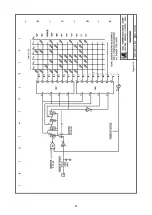
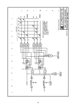
Page 99: ...ne of a series of logic gates which actuates the appropriate character sequencer in the keyboard Characters or keystrokes from the keyswitch board enter the buffer whenever the READY line from the key...

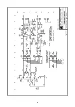
Page 100: ...A5...

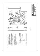
Page 101: ...A6...

Reviews: