Subject to change without notice
9
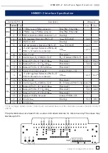
H M 8 0 0 1 - 2 I n t e r f a c e S p e c i f i c a t i o n
Connector-Pin
Description
Voltage at
Bottom Top
I
min
I
max.
BNC
1
23 1
st
BNC- resp. 4
th
BNC-connector
(Only PIN1; PIN 23 NC)
2
24 2
nd
BNC- resp. 3
rd
BNC-connector
(Only PIN2; PIN 24 NC)
3
25 GND-connection of BNC-connector 1 + 2
(fl oating)
U1
4
26 +5 V regulated. Reference PIN 5 + 27;
1 A
max
[
Σ
(5 V, 8 V)]
5.0 V
5
27 GND (5 V + 8 V)
(fl oating)
0.0 V
6
28 +8 V not regulated. Reference PIN 5 + 27;
1 A
max
[
Σ
(5 V, 8 V)]
14.6 V
U2
7
29
+5...20 V regulated. Reference PIN 8 + 30;
PIN 11 + 13 need to be connected.
0.5 A
max
16.9 V
16.9 V *)
8
30 GND +5…20 V
(Potential 2)
9
31 Control input
;
R
Ci
=18.8/(Ua -5.2 V)
(R
Ci
= R between PIN 8 + 9)
1.62 k
Ω
*)
U2a
10
32 Between Pin 10 + 11; 18 V
AC
0.8 A
max
(Potential 2)
20.7 V
19.2 V
11
33 Between Pin 11 + 12; 7 V
AC
0.8 A
max
(Potential 2)
7.0 V
6.6 V
12
34 Between Pin 10 + 12 25 V
AC
0.8 A
max
(Potential 2)
27.7 V
13
35 Supply of U2 (U2a not used)
(connect PIN 11 + 13)
U3
14
36
+5...20 V regulated. Reference PIN 15 + 37.
PIN 18 + 20 need to be connected.
0.5 A
max
16.6 V
16.6 V *)
15
37 GND +5…20 V
(Potential 3)
16
38 Control input;
R
Ci
=18.8/(Ua -5.2 V)
(R
s
= R between PIN 15 + 16) 1.62 k
Ω
*)
U3a
17
39 Between Pin 17 + 18; 18 V
AC
0.8 A
max
(Potential 3)
20.6 V
19.3 V
18
40 Between Pin 18 + 19; 7 V
AC
0.8 A
max
(Potential 3)
7.0 V
6.6 V
19
41 Between Pin 17 + 19; 25 V
AC
0.8 A
max
(Potential 3)
27.6 V
20
42 Supply of U3 (U3a not used)
(connect PIN 18 + 20)
U4
21
43 8 V
AC
0.4 A
max
(fl oating)
9.3 V
8.8 V
22
44 8 V
AC
0.4 A
max
HM8001-2 Interface Specifi cation
*) The voltages shown in line 7 and 14 are calculated based on the resistance values choosen in line 9
and 16.
The provided values are taken from a series instrument and are for reference only. The values may
deviate up to 5%.


