©1998 Hamtronics, Inc.; Hilton NY; USA. All rights reserved. Hamtronics is a registered trademark. Revised: 12/11/02
- Page 2 -
PARTS LIST FOR R301
RECEIVER.
☞
Note: Values which vary with freq. band
are shown in a table at the end of the parts list.
Capacitors are disc type unless noted other-
wise.
➊
Resistors used as test point or external
connection point. These must be installed on
the board oriented properly and with the top
loop an extra 1/6” high to allow for connections
to the loop later. (See detail in component lo-
cation diagram.)
➋
Microcontroller must be factory pro-
grammed for proper band segment and for
TCXO or crystal osc option.
➌
This part must be installed with a small
space (about the thickness of an index card)
under the part to prevent the bottom of the part
from shorting to the ground plane.
0
Caution: IC’s are static sensitive. Use
appropriate handling precautions to avoid dam-
age.
Ref Desig Value (marking)
C1 not
used
C2
0.1µf monolithic (104)
C3
.001 uf (102, 1nM, or 1nK)
C5-C7 not
assigned
C8
.001 uf (102, 1nM, or 1nK)
C9
0.1µf monolithic (104)
C10 0.15µf
mylar
(red)
C11 .022µf
mylar
(223)
C12
.0022µf (2.2nK or 222)
C13 not
assigned
C14 10µf
electrolytic
C15
0.1µf monolithic (104)
C19 10µf
electrolytic
C22 4pf
C26 2pf
C32 not
used
C34 not
used
C36 4pf
C40 .01µf
(103)
C41 5pf
C42 6pf
C43 5pf
C44 0.47µf
electrolytic
C45 0.15µf
mylar
(red)
C46-C47 .001 uf (102, 1nM, or 1nK)
C48 0.15µf
mylar
(red)
C49-C50 .01µf
(103)
C51 470µf
electrolytic
C52 10µf
electrolytic
C53 1µf
electrolytic
C54 100µf
electrolytic
C55 not
used
C56 220pf
(221)
C57 68pf
C58-C61 0.1µf monolithic (104)
C62-C63 not
used
C64
10 µf electrolytic
C65 100
µf
electrolytic
D1
BB132 varactor diode
(surface mt under board)
D2-D4
1N4148 switching diode
FL1-FL4
➌
10.7MHz crystal filter
(matched set of 4)
FL5
455kHz ceramic filter
J1 RCA
Jack
L2
0.33µH RF choke
(red-sil-orn-orn)
L3-L8
2½ t. ,slug tuned (red)
L9
0.33µH RF choke
(red-sil-orn-orn)
Q1-Q2 2N5770
Q3 2N3904
Q4-Q5
BF998 MOS FET (surface
mount under board)
Q6 2N5770
Q7 2N3904
R1 180
Ω
R2 not
used
R3 not
assigned
R4 47K
R5 15K
R6
➊
47K
R7
not assigned
R8 2.2K
R9 10K
R10 6.8K
R11 3.9K
R12 180
Ω
R13 47
Ω
R14 47K
R15 470
Ω
R16
➊
3.9meg
R17-R18 100K
R19
➊
47K
R20 330K
R21 15K
R22 47K
R23
100K panel mount pot.
R24 47K
R25 100K
R26
➊
47K
R27 330K
R28 4.7K
R29 680
Ω
R30 1.2K
R31
➊
22K
R32
100K panel mount pot.
R33 2.2K
R34 4.7K
R35 47K
R36 330K
R37 3.9meg
R38 2meg
R39 180
Ω
R40 27
Ω
S1
10 pos. DIP switch
T1
10.7MHz IF xfmr
(7A-691F)
T2
455kHz IF transformer
(T1003)
U1
0
➋
MC68HC705J1A
µP
U2
0
MC145190F
(surface mt under board)
U3
0
10.240 MHz TCXO
U4
MC3361BP IF ampl
U5 LM380N-8
af
output
U6 78L08
regulator
Y2
➌
10.245
MHz
crystal
Z1-Z3 Ferrite
bead,
prestrung
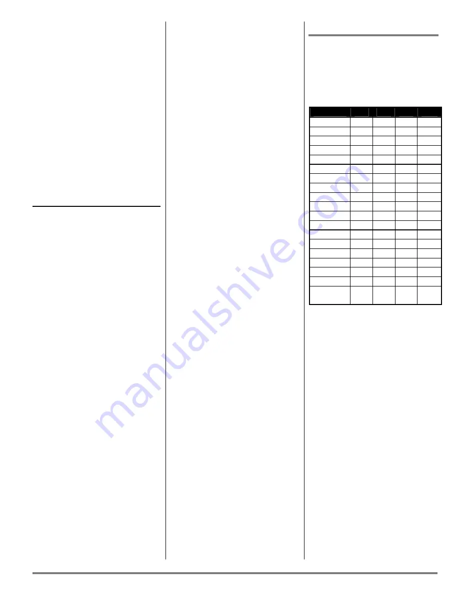
VALUES WHICH VARY WITH
FREQUENCY BAND:
R301-2 is 144.000 - 154.235 MHz
R301-3 is 154.200 - 164.435 MHz
R301-4 is 164.400 - 174.635 MHz
R301-5 is 216.000 - 226.235 MHz
R301-6 is 220.000 - 230.235 MHz
Ref Desig
-2
-3
-4
-5/-6
C4
10 10 10 n/u
C16 10 10 10
8
C17,
C18 .001 .001 .001 220
C20 12
10
8
11
C21 68 62 47 47
C23
.001 .001 .001 100
C24 27 22 18 8
C25 62 47 47 27
C27
220 220 220 100
C28 20 18 15 5
C29 56 47 43 15
C30
220 220 220 100
C31 18 15 12 6
C33 20 18 15 7
C35 15 15 12 4
C37 27 22 20 9
C38 82 62 56 27
C39 10
8 8 3
L1 2½T
(red)
2½T
(red)
2½T
(red)
1½T
(brn)


