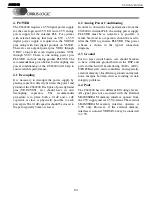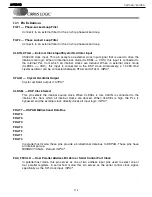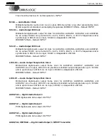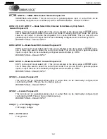
from either an external microcontroller or through
one of the boot procedures listed in Section 8.
3. TYPICAL CONNECTION DIAGRAMS
Four typical connection diagrams have been
presented to illustrate using the part with the
different communication modes available. They
are as follows:
Figure 27, "SPI Control with External Memory -
144 Pin Package" on page 38.
Figure 28, "Intel
®
Parallel Control Mode - 144 Pin
Package" on page 39.
Figure 29, "Motorola
®
Parallel Control Mode - 144
Pin Package" on page 40.
The following should be noted when viewing the
typical connection diagrams:
Note:
The pins are grouped functionally in each
of the typical connection diagrams. Please be
aware that the CS49400 symbol may appear
differently in each diagram.
The external memory interface is supported
when a serial or parallel communication mode
has been chosen.
3.1 Multiplexed Pins
The CS49400 incorporates a large amount of
flexibility into a 144 pin package. The pins are
internally multiplexed to serve multiple purposes.
Some pins are designed to operate in one mode at
power up, and serve a different purpose when the
DSP is running. Other pins have functionality
which can be controlled by the application running
on the DSP. In order to better explain the behavior
of the part, the pins which are multiplexed have
been given multiple names. Each name is specific
to the pin’s operation in a particular mode.
In this document, pins will be referred to by their
functionality.
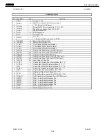
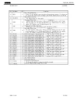
Section 12
“Pin Description” on
page 86
describes each pin of the CS49400 and lists
all of its names. Please refer to this section when
exact pin numbers are in question.
3.2 Termination Requirements
The CS49400 incorporates open drain pins which
must be pulled high for proper operation.
FINTREQ and INTREQ are always open drains
which requires a pull-up for proper operation.
Due to the internal, multiplexed design of the pins,
certain signals may or may not require termination
depending on the mode being used. If a parallel
host communication mode is not being used, all
parallel control pins must be terminated or driven
as these pins will come up as high impedance
inputs and will be prone to oscillation if they are
left floating. The specific termination requirements
may vary since the state of some of the GPIO pins
will determine the communication mode at the
rising edge of reset (please see
Section 6 “Control”
on page 41
for more information). For the explicit
termination requirements of each communication
mode please see the typical connection diagrams.
Generally a 3.3k Ohm resistor is recommended for
open drain and mode select pins. A 10k Ohm
resistor is sufficient for all other unused inputs.
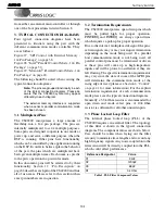
3.3 Phase Locked Loop Filter
The internal phase locked loop (PLL) of the
CS49400 requires an external filter. The topology
of this filter is shown in the typical connection
diagrams. The component values are shown below.
Care should be taken when laying out the filter
circuitry to minimize trace lengths and to avoid any
high frequency signals. Any noise coupled onto the
filter circuit will be directly coupled into the PLL,
which could affect performance.
Reference Designator
Value
C1
2.2uF
C2
1200pF
C3
68pF
R1
3k Ohm
Table 1. PLL Filter Component Values
AVR340
harman/kardon
108
Summary of Contents for AVR 340
Page 33: ...AVR340 harman kardon 33...
Page 35: ...AVR340 harman kardon 35...
Page 80: ...AVR340 harman kardon...
Page 81: ...AVR340 harman kardon...
Page 82: ...AVR340 harman kardon 82...
Page 83: ...CAM350 PRO V 7 6 Mon Sep 01 10 29 56 2003 Untitled AVR340 harman kardon 83...
Page 84: ...AVR340 harman kardon 84...
Page 85: ...AVR340 harman kardon 85...
Page 123: ...AVR340 harman kardon 123...
Page 124: ...AVR340 harman kardon 124...
Page 125: ...AVR340 harman kardon 125...
Page 126: ...AVR340 harman kardon 126...
Page 129: ...AVR340 harman kardon 129...
Page 130: ...AVR340 harman kardon 130...
Page 131: ...AVR340 harman kardon 131...
Page 132: ...AVR340 harman kardon 132...
Page 133: ...AVR340 harman kardon 133...
Page 134: ...AVR340 harman kardon 134...
Page 135: ...AVR340 harman kardon 135...
Page 136: ...AVR340 harman kardon 136...
Page 137: ...AVR340 harman kardon 137...
Page 139: ...TC90A49P F BLOCK DIAGRAM PIN ASSIGNMENT AVR340 harman kardon 139...
Page 148: ...AVR340 harman kardon 148...
Page 151: ...LC74763M BLOCK DIAGRAM AVR340 harman kardon 151...
Page 158: ...AVR340 harman kardon 158...
Page 159: ...AVR340 harman kardon 159...
Page 162: ...AVR340 harman kardon 162...
Page 166: ...AVR340 harman kardon 166...
Page 167: ...AVR340 harman kardon 167...
Page 168: ...AVR340 harman kardon 168...
Page 169: ...AVR340 harman kardon 169...
Page 170: ...AVR340 harman kardon 170...
Page 171: ...AVR340 harman kardon 171...
Page 172: ...AVR340 harman kardon 172...
Page 173: ...AVR340 harman kardon 173...
Page 176: ...AVR340 harman kardon 176...
Page 178: ...AVR340 harman kardon 178...
Page 179: ...SCHEMATIC sch 1 Fri Oct 21 10 53 55 2005 AVR340 harman kardon 179...
Page 180: ...LPP 051021 sch 1 Fri Oct 21 10 40 28 2005 AVR340 harman kardon 180...
Page 181: ...NPUT LPP 051021 sch 2 Fri Oct 21 10 42 09 2005 AVR340 harman kardon 181...
Page 182: ...UT LPP 051021 sch 3 Fri Oct 21 10 43 03 2005 AVR340 harman kardon 182...
Page 183: ...EMATIC sch 1 Fri Oct 21 10 52 43 2005 AVR340 harman kardon 183...
Page 184: ...CHEMATIC sch 1 Fri Oct 21 10 56 51 2005 AVR340 harman kardon 184...
Page 185: ...SCHEMATIC sch 2 Thu Oct 27 15 39 31 2005 AVR340 harman kardon 185...
Page 186: ..._0810 sch 1 Wed Aug 10 16 28 25 2005 AVR340 harman kardon 186...

